下载:
下载:


-
大口径的高斜率动态范围光学元件在光学系统中具有改善成像品质、减少光能损失[1]等优点,被广泛应用于光学成像、照明和医疗影像等领域。此类光学元件具有面形复杂、斜率范围大的特性,对其加工制造及检测技术提出了更高的要求。目前面形的非接触式检测技术主要包括干涉法[2]与几何光线法。其中,干涉检测法包括光学干涉仪、全息测量法和倾斜波前法等。光学干涉仪作为一种非接触式测量方法,具有高检测精度及高空间分辨率的优点,但其动态范围较小且易受环境扰动影响。全息测量法[3]的测量精度较高,但其一对一的补偿测量模式导致其检测成本高、通用性差。倾斜波前法[4]可实现大动态范围的高精度检测,但该测量法检测过程复杂、且测量口径有限。几何光线法包括夏克-哈特曼波前探测法、光学偏折技术等。夏克-哈特曼波前探测法[5]需借助透镜阵列来实现波前检测,故而受透镜尺寸和数目的限制,其动态范围较小、横向分辨率不高。光学偏折技术[6-7]具有检测精度较高、动态测量范围较大以及系统结构简单等优点,在各类球面、非球面甚至自由曲面光学元件测量中得到了广泛应用。
为了进一步实现大口径光学元件的面形检测,子孔径拼接测量技术[8]应运而生。子孔径拼接的基本原理[9]是将被测面形划分为多个相对较小的子孔径区域,将测量得到的各个子孔径数据进行拼接,从而获取全口径面形。目前子孔径拼接术通常按照圆形或环形等规则形状对全口径面形进行划分[10-11],但是在对高斜率动态范围光学元件进行测量时,圆形或环形等规则形状的子孔径划分拼接法灵活性较差、拼接效率不高。
为了满足大口径的高斜率动态范围光学反射元件的测量需求,文中提出基于光学偏折技术的子孔径拼接测量方法。根据被测元件的曲面特征进行子孔径划分,并利用所搭建的条纹投影光学偏折测量系统对各子孔径进行测量,由各子孔径实际光斑分布与理想光斑分布偏差重构得到其面形数据,进而可对各子孔径面形数据进行拼接,由此获取全口径面形测量结果。由于光学偏折测量技术相对干涉法具有很大的测量动态范围和视场,可极大降低所需的子孔径数量,由此大大提高了检测效率。同时提出了基于子孔径重叠区域位姿的加权融合算法,改善了拼接面形的“拼接痕迹”。为验证所提方法的可行性,进行了仿真分析和实验验证。对一反光灯罩进行拼接测量,并将最终拼接测量结果与全口径测量结果进行对比分析。该测量方法具有测量精度较高、动态测量范围大以及系统结构简单等特点,可满足大口径的高斜率动态范围光学元件的检测需求。
-
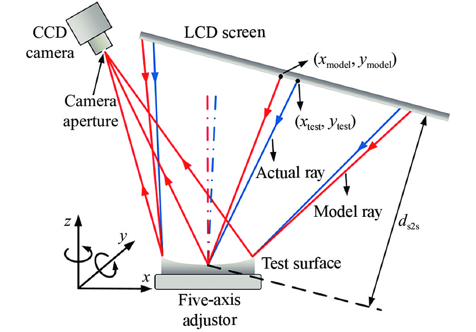
基于光学偏折技术的子孔径拼接测量系统原理图如图1所示,系统组成部分包括LCD投影屏、CCD相机、被测元件以及子孔径扫描机构。在图1所示的条纹投影偏折测量系统中,利用LCD投影屏将编码正弦条纹投射到被测反射元件表面,并通过CCD相机采集经被测元件表面反射后的变形条纹。利用五轴调整架作为子孔径扫描机构,通过调节被测元件位置来实现各个测量子孔径区域的调整,由此实现被测元件全口径覆盖。在各个子孔径区域测量中,LCD投影屏上的发光像素点、被测区域投影位置与CCD相机上亮点像素之间存在一一对应关系,可据此确定各入射光线与对应的反射光线,以此计算得到被测面形的投影位置在x和y方向的斜率,进而实现被测元件的面形测量。
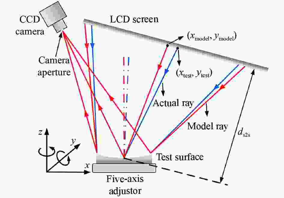
图 1 基于光学偏折技术的子孔径拼接测量系统原理图
Figure 1. Schematic diagram of optical deflectometric system for sub-aperture stitching measurement
按照实际测量系统的结构参数可建立对应的系统光线追迹模型,由此获得接收像面上的理想光斑分布(xmodel, ymodel);在实际测量中,利用条纹相移技术测得被测面形在投影屏上的实际光斑分布(xtest, ytest)。被测面相对其理想面的斜率偏差(∆wx, ∆wy)可通过理想光斑分布(xmodel, ymodel)与实际光斑分布(xtest, ytest)的坐标偏差(∆xspot, ∆yspot)计算得到,即
$$\left\{ \begin{gathered} \Delta {w_x} = \frac{{\partial W\left( {x,y} \right)}}{{\partial x}} = \frac{{{x_{{\rm{test}}}} - {x_{{\rm{model}}}}}}{{2{d_{{\rm{s2s}}}}}} = \frac{{\Delta {x_{{\rm{spot}}}}}}{{2{d_{{\rm{s2s}}}}}} \\ \Delta {w_y} = \frac{{\partial W\left( {x,y} \right)}}{{\partial y}} = \frac{{{y_{{\rm{test}}}} - {y_{{\rm{model}}}}}}{{2{d_{{\rm{s2s}}}}}} = \frac{{\Delta {y_{{\rm{spot}}}}}}{{2{d_{{\rm{s2s}}}}}} \\ \end{gathered} \right.$$ (1) 式中:ds2s为被测元件与投影屏的距离;(x, y)为测量系统出瞳面上的坐标;W(x, y)为被测面引入的波前像差。根据公式(1)可求得实际面形与其理想面形的斜率偏差(∆wx, ∆wy),通过对斜率偏差(∆wx, ∆wy)进行表面积分,即可获得被测元件的面形信息。
-
图1所示的光学偏折测量系统最大可测的斜率范围∆L与LCD投影屏的尺寸、系统孔径有关,并且有
$$\Delta L = {L_{\rm screen}}/2{d_{\rm s2s}}$$ (2) 式中:Lscreen为LCD投影屏的实际有效尺寸。因此可以通过增大LCD投影屏的有效尺寸以及调整被测元件与LCD投影屏、CCD相机之间相对距离的方式,实现对更大口径及更高斜率动态范围光学元件表面的测量。但是当被测元件的口径及斜率动态范围过大而超出系统可测范围时,依旧存在无法实现全口径测量的问题。此时可对被测元件各部分区域(子孔径)进行测量,再将其拼接得到全口径面形。
在CCD相机的视场范围中,通过调整五轴调整架来改变被测元件的位姿,使被测面形部分区域的变形条纹保持在合理的密集度。在当前位姿状态下,可同时利用五轴调整架对被测元件进行子孔径扫描,再通过CCD相机逐次采集各子孔径数据,直至覆盖全口径面形。在子孔径划分设计中应遵循子孔径间重叠区域大于子孔径区域的1/4,同时子孔径的数目尽量少的原则[12]。
实际测量中,由于被测元件的移动会导致不同子孔径之间产生倾斜、平移和离焦误差。因此需要计算各子孔径之间对应的倾斜、平移与离焦系数,将各个子孔径数据变换到统一坐标下进行拼接处理。对于任意两个重叠区域的子孔径,其面形之间的关系可表示为:
$$ {w_m}(x,y) - {w_n}(x,y) {\rm{ = }}{A_{m{\rm{,}}n}}x + {B_{m{\rm{,}}n}}y + {C_{m{\rm{,}}n}}\left( {{x^{\rm{2}}}{\rm{ + }}{y^{\rm{2}}}} \right) + {D_{m{\rm{,}}n}} $$ (3) 式中:wm(x, y)与wn(x, y)分别表示第m、n个子孔径的面形数据;Am, n和Bm, n分别表示第m个子孔径相对于第n个子孔径在x、y方向的倾斜系数;Cm, n和Dm, n分别为其对应的离焦系数和平移系数。根据最小二乘拟合法,在子孔径间的重叠区域面形平方和最小条件下,可求取各子孔径间的倾斜、平移与离焦系数,即
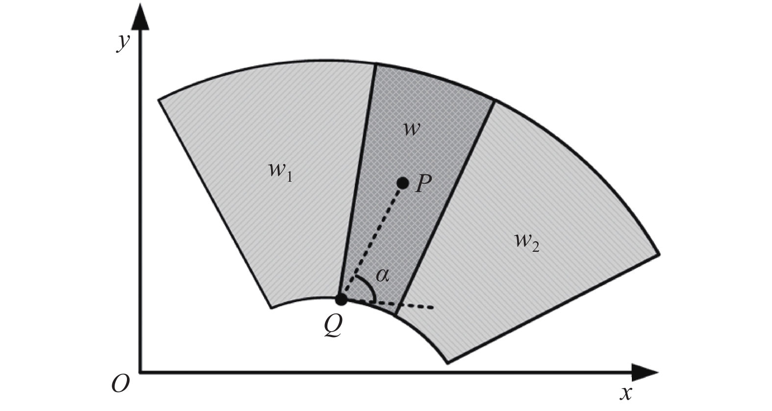
$$\begin{split} {\rm{min}} =& \sum\limits_m {\sum\limits_n^{m \cap n} {\left\{ {{w_m}(x,y) - {w_n}(x,y) - } \right.} } \\& {A_{m{\rm{,}}n}}x - {B_{m{\rm{,}}n}}y - {C_{m{\rm{,}}n}}({x^{\rm{2}}}{\rm{ + }}{y^{\rm{2}}}) - {\left. {{D_{m{\rm{,}}n}}} \right\}^2} \end{split} $$ (4) 在重叠区域数据的计算处理中,利用传统均值计算法获取的拼接面形难免会产生“拼接痕迹”。为实现拼接面形的平滑过渡,可采用基于子孔径重叠区域位姿的加权融合算法。以图2所示的任意两个具有重叠区域的子孔径为例,以该重叠区域的质点P与距质点最远点Q两点间连线
$PQ$ 和x轴正半轴夹角的绝对值α作为任一子孔径位姿方位角的表征值。
图 2 两子孔径及其重叠区域示意图
Figure 2. Diagram of two sub-apertures and their overlapped region
根据子孔径相对于x轴的位姿分布特征,可设定方位临界值α0(如α0 = π/4),当方位角α > α0时,取在重叠区域任一横坐标区间[x1, x2]内渐变系数为kx;当方位角α ≤ α0时,取在重叠区域任一纵坐标区间[y1, y2]内渐变系数为ky。其中kx、ky的取值范围均为[0, 1],并且有
$$\left\{ \begin{gathered} {k_x} = 0.5 - 0.5\cos \left( {\frac{{x - {x_1}}}{{{x_2} - {x_1}}}} \right)\pi \\ {k_y} = 0.5 - 0.5\cos \left( {\frac{{y - {y_{\rm{1}}}}}{{{y_2} - {y_1}}}} \right)\pi \\ \end{gathered} \right.$$ (5) 因此,两子孔径间重叠区域的面形w可表示为:
$$ w=\left\{ {\begin{array}{*{20}{c}} {\left(1-{k}_{x}\right){w}_{1}+{k}_{x}{w}_{\rm{2}},\;\;{\rm{if}}\;\;\alpha \leqslant {\alpha }_{0}}\\ {\left(1-{k}_{y}\right){w}_{1}+{k}_{y}{w}_{2},\;\;{\rm{if}}\;\;\alpha >{\alpha }_{0}} \end{array}} \right.$$ (6) 式中:w1、w2分别为任意两个子孔径在重叠区域内的面形数据。由公式(5)和公式(6)可得,任一重叠区域内的渐变系数变化趋势均为平滑上升的曲线[13],因而能够有效避免重叠区域边缘点突变导致的“拼接痕迹”。当渐变系数为kx时,由kx的变化趋势可得,越靠近重叠区域任一区间端点x1时造成“拼接痕迹”的面形数据w1的权重越低,越靠近重叠区域任一区间端点x2时造成“拼接痕迹”的面形数据w2的权重越低;当渐变系数为ky时,同理如上。利用上述处理方法可以改善“拼接痕迹”,实现拼接面形的平滑过渡。
-
为验证所提出方法的可行性,对其进行仿真分析。利用光线追迹方法建立对应的子孔径光学偏折测量系统,仿真中被测对象为一非球面(抛物面)反射镜,其圆锥系数为−1,顶点球半径为30 mm,内口径为4.7 mm,外口径为14 mm,同时附加了一个以Zernike多项式进行表征的面形偏差。按照子孔径划分原则,将被测面形划分为6个子孔径,各子孔径的面形数据及其在全局位置的分布图如图3所示。
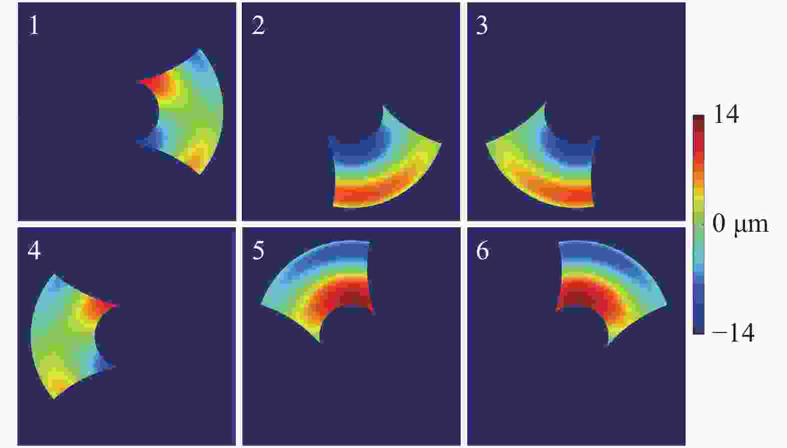
图 3 仿真中子孔径面形数据及其全局位置分布
Figure 3. Surface data and its global position for various sub-apertures in simulation
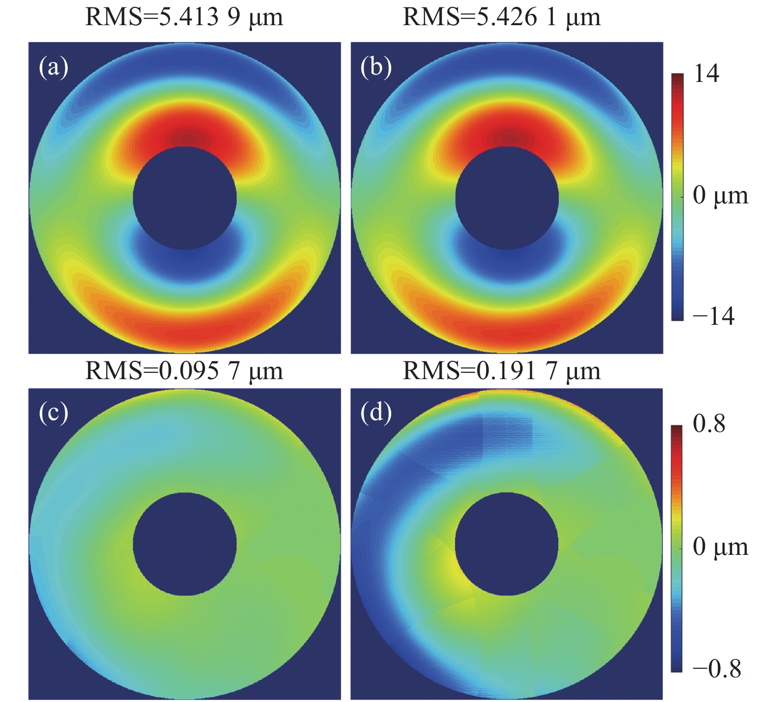
利用所提出基于加权融合的拼接算法对各子孔径进行拼接,最终得到的拼接面形如图4(a)所示,被测元件的真实名义面形如图4(b)所示,其中文中所述方法获取的拼接面形的RMS与PV值分别为5.4139 µm和24.1762 µm,真实面形的RMS与PV值分别为5.4261 µm和24.2264 µm,两者对应的残差分布如图4(c)所示,其RMS与PV值分别为0.0957 µm和0.6762 µm。同时传统均值计算拼接法[14]获取的拼接面形与真实面形的残差分布如图4(d)所示,其RMS与PV值分别为0.1917 µm和1.6295 µm。由图4可知,利用文中所提出拼接方法获取的全口径面形与全口径真实面形结果在面形形状和数量值上均具有良好的一致性,并且其残差分布效果明显优于传统均值计算法的残差分布。
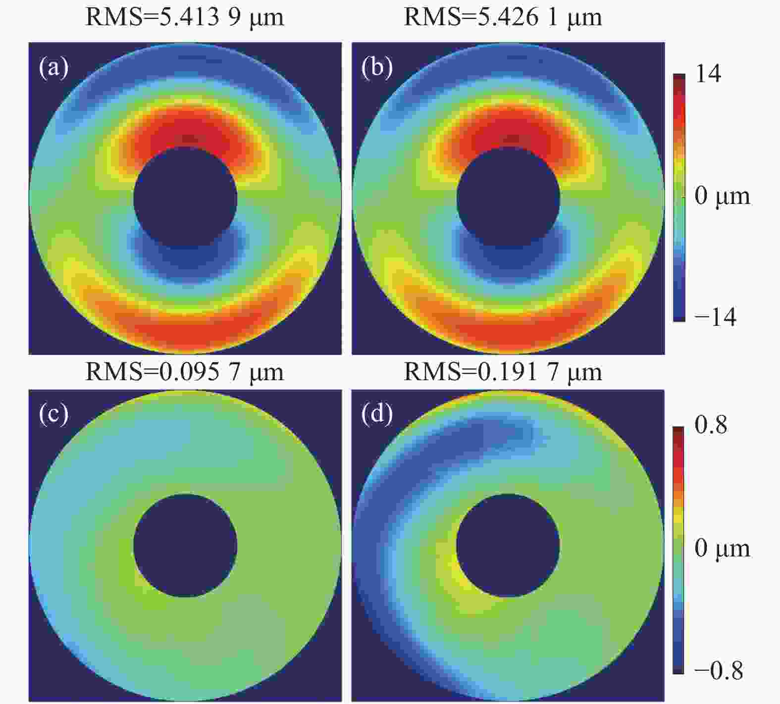
图 4 仿真中拼接面形与残差分布。(a) 基于加权融合拼接法获取的拼接面形;(b) 真实面形;(c) 图(a)与图(b)的残差分布;(d) 均值计算法获取的拼接面形与真实面形残差分布
Figure 4. Stitched surfaces and residual errors in simulation. (a) Stitched surface with weighted-fusion method; (b) Nominal surface; (c) Residual error between (a) and (b); (d) Residual error between stitched surface based on mean calculation method and nominal surface
-
基于光学偏折技术的子孔径拼接测量系统中影响面形测量精度的主要误差因素包括:子孔径定位误差、相机畸变、投影屏的非线性输出以及形变误差、系统结构误差等。
子孔径定位误差主要是由子孔径扫描平台运动误差引起的。可通过对任两个子孔径在重叠区域内面形数据的显著特征进行匹配定位,来减少子孔径位置的误差偏移量[12]。CCD相机的成像畸变可通过张正友标定法[15],获取相机的畸变参数进行校正。为满足人眼的主观感知,LCD投影屏对灰度值的输出显示通常会呈现非线性变化,可通过查表法来解决LCD投影屏非线性输出的问题。同时LCD投影屏的表面形状会在重力因素及加工安装误差的影响下出现变形,可通过三坐标测量机对其标定测量实现误差校正。系统结构误差来自对测量系统结构参数(用于光线追迹建模)的标定误差,利用计算机辅助的结构误差校正方法[6]可对其进行有效抑制,并可实现纳米量级的检测精度。
-
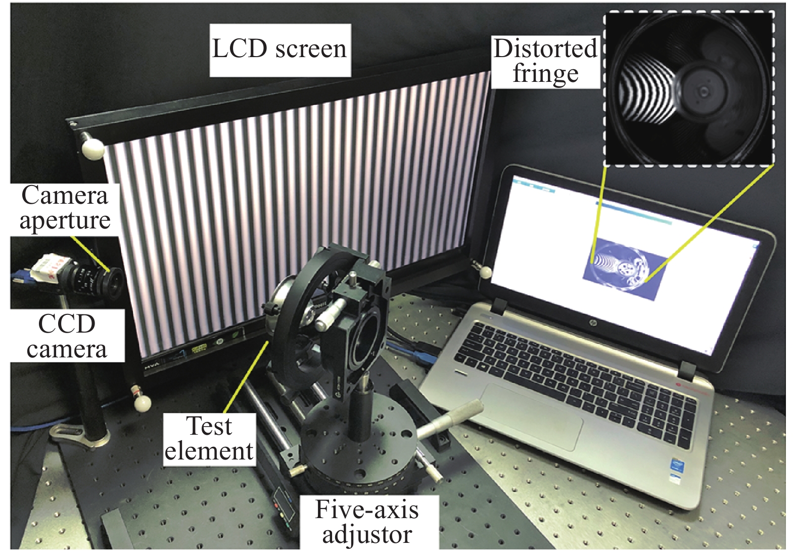
为验证文中所提基于光学偏折技术的子孔径拼接测量方法的可行性,搭建了图5所示的子孔径拼接测量实验系统。其中,LCD投影屏的分辨率为1920×1080,像元尺寸为0.265 mm×0.265 mm;CCD相机的分辨率为1328×1048,像元尺寸为3.63 µm×3.63 µm;五轴调整架的平移定位误差约为0.03 mm,旋转定位误差约为0.02°。被测对象是一个内、外口径分别约为30 mm和58 mm,高度约为28 mm的反光灯罩。
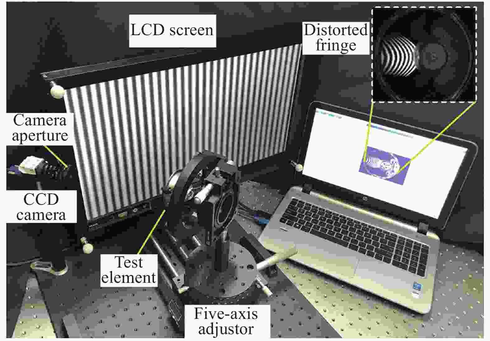
图 5 基于光学偏折技术的子孔径拼接测量实验系统
Figure 5. Experimental setup of optical deflectometric system for sub-aperture stitching measurement
实验中通过五轴调整架调节被测元件与LCD投影屏、CCD相机的相对位置,使装有前置针孔的CCD相机能够对最大区域的待测元件进行清晰成像。图6(a)和图6(b)分别为CCD相机采集到的x、y方向变形条纹图。在当前位置状态下,通过五轴调整架旋转被测元件,使得CCD相机可以逐个采集经被测元件各子孔径反射的变形条纹。

图 6 CCD相机采集的变形条纹图
Figure 6. Distorted fringes patterns acquired with CCD camera
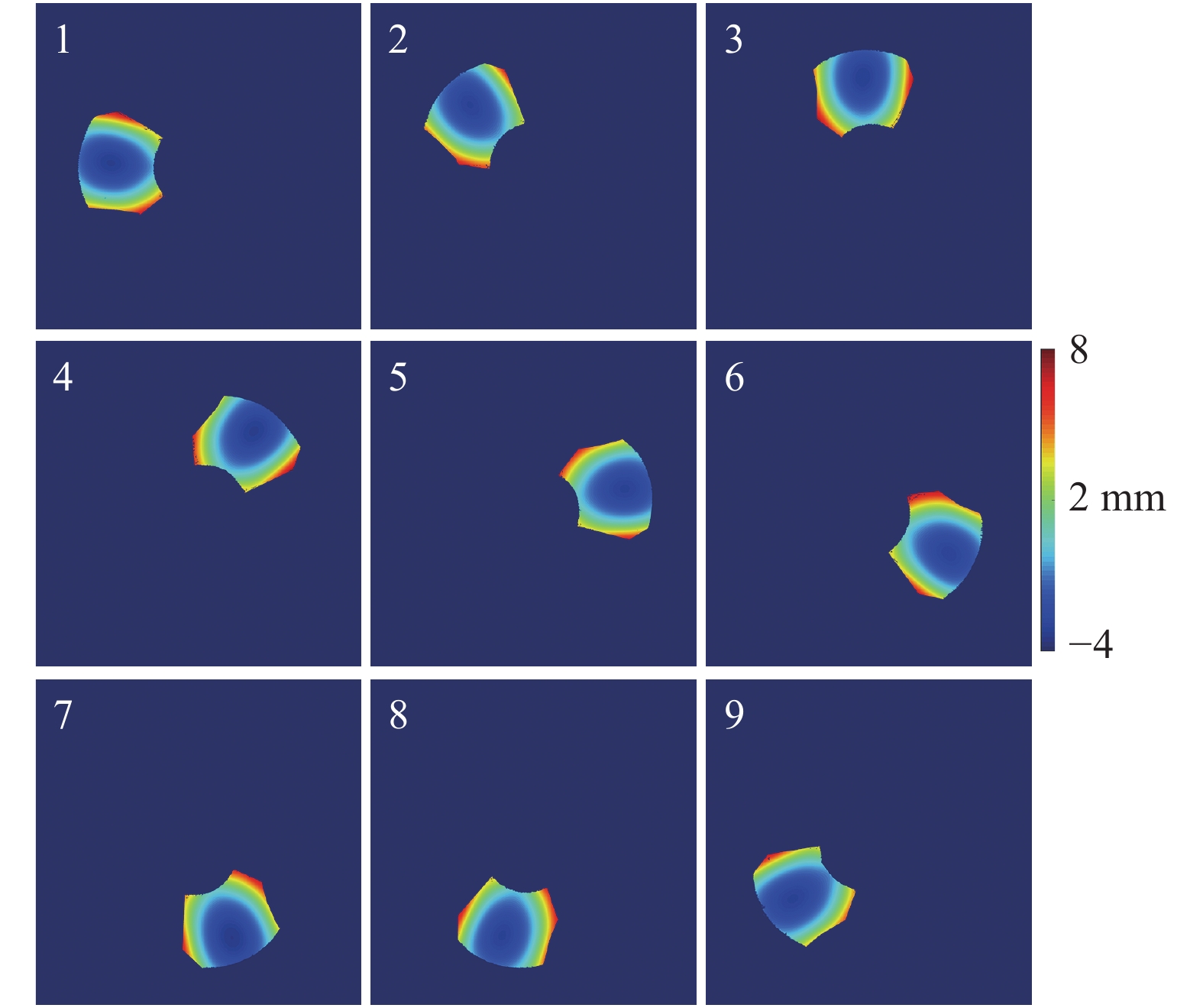
通过三坐标测量机(Hexagon Global Classic,测量精度1.7 µm)对测量系统各器件的位置结构参数进行预标定,其中反光灯罩内口径几何中心到LCD投影屏、CCD相机前置小孔间的距离分别约为187.1167 mm和195.2958 mm。根据预标定结果获得的测量系统结构参数,建立对应的系统光线追迹模型,以此可消除系统结构误差并计算得到各个子孔径对应面形数据。图7所示为获取的9个子孔径面形数据及其在全局位置的分布。

图 7 实验中测得子孔径面形及其全局位置分布
Figure 7. Measured surface and its global position for various sub-apertures in experiment
利用文中所提基于加权融合的子孔径拼接法对各子孔径进行拼接,最终获取的全口径拼接测量结果如图8(a)所示(此处为了便于后续数据对比,对测量结果进行了高度方向坐标取反转换),其对应的RMS和PV值分别为7.652 7 mm和27.532 4 mm。为验证文中拼接测量的有效性,同时进行了比对实验。由于目前尚没有高精度的大动态范围商业测量仪器可对实验对象直接进行非接触式全口径测量,比对实验中采用激光扫描仪(BYSCAN750LE,精度为0.02 mm)对反光灯罩进行了测量,图8(b)所示为所测得的全口径测量结果,其RMS和PV值分别为7.646 3 mm和27.520 8 mm,相对于基于光学偏折技术的子孔径拼接测量结果RMS值偏差为0.006 4 mm。两者测得面形对应的残差分布见图8(c),其RMS值为0.011 3 mm。利用传统均值计算拼接法获取的拼接测量结果与全口径测量结果的残差分布如图8(d)所示,其RMS值为0.014 8 mm。由图8可以看出,利用文中所提基于光学偏折技术的子孔径拼接测量系统获取的拼接测量结果与扫描仪全口径测量结果在面形形状上基本吻合,在量值上具有较好的一致性;且与传统均值计算拼接法相比,文中所提方法获取的拼接面形平滑、无子孔径“拼接痕迹”,且其残差分布在RMS与PV值上明显优于传统均值计算拼接法的残差分布。需要指出的是,由于激光扫描仪的测量精度有限,同时面形残差计算过程中全口径测量数据与子孔径扫描拼接测量结果位置难以完全匹配,进而导致残差计算结果相对于理论精度量值偏大。
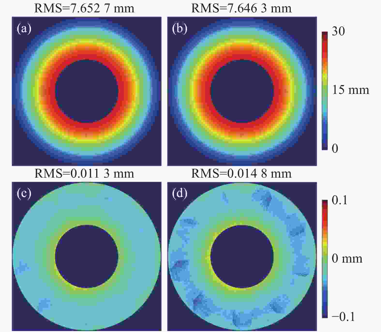
图 8 实验中反光灯罩全口径测量结果与残差分布。(a) 基于加权融合拼接法的测量结果;(b) 激光扫描仪测量结果;(c) 图(a)与图(b)的残差分布;(d) 均值计算拼接法的测量结果与扫描仪测量结果残差分布
Figure 8. Full-aperture measurement results and residual errors for a reflective lampshade in experiment. (a) Measurement result with weighted-fusion method; (b) Measurement result with a laser scanner; (c) Residual error between (a) and (b); (d) Residual error between measurement result stitched with mean calculation method and that with laser scanner
-
为满足大口径的高斜率动态范围光学元件的测量,提出了一种基于光学偏折技术的子孔径拼接测量方法。搭建了条纹投影光学偏折测量实验系统,通过被测元件的曲面特征进行子孔径划分,利用子孔径扫描机构调整被测元件的位姿,并通过CCD相机逐次获取各子孔径区域内经被测元件反射的变形投影条纹。同时按照预标定获得的结构参数建立对应的测量系统模型并进行光线追迹,由实际测量结果与光线追迹结果的偏差重构各子孔径的面形数据,在此基础上对其进行拼接,最终实现全口径面形拼接测量。同时提出了重叠区域的加权融合算法来实现拼接面形的平滑过渡。对所提出的方法分别进行了仿真分析与实验测量,通过与全口径测量结果的比对,结果表明文中所述方法具有较高的检测精度,且明显优于传统均值计算的拼接结果;其中,在仿真分析中文中所述方法获取的拼接面形与全口径真实面形的RMS和PV值偏差分别为0.0957 µm和0.6762 µm,该拼接测量系统具有较高的检测精度与大动态测量范围且系统结构简单,为大口径的高斜率动态范围光学反射元件的检测提供了一种有效可行的方法。
Sub-aperture stitching deflectometric testing technology for optical surfaces
-
摘要: 针对大口径的高斜率动态范围光学元件的测量需求,提出了基于光学偏折技术的子孔径拼接测量方法。利用所搭建的条纹投影光学偏折测量系统,结合子孔径划分拼接方法,对各子孔径分别进行测量,并根据实际测量结果与测量系统模型光线追迹结果的偏差,高精度测得各个子孔径的面形数据,由此对各子孔径进行拼接来实现全口径面形测量。光学偏折测量技术相对干涉法具有很大的测量动态范围和视场,可极大降低所需的子孔径数量,由此大大提高了检测效率。同时提出了针对重叠区域的加权融合算法来实现拼接面形的平滑过渡。为验证所提出方案的可行性,分别进行了仿真分析以及实验验证。对一高斜率反光灯罩进行拼接测量实验,并将拼接测量与全口径测量结果进行对比。结果表明,利用所提出测量方法获得的拼接面形连续光滑,且与全口径测量面形RMS值偏差为0.0957 µm,优于微米量级。该测量具有较高的测量精度和大动态测量范围,并且系统结构简单,为各类复杂光学反射元件提供了一种有效可行的检测方法。Abstract: Aiming at the measurement needs of large-aperture optical elements with ultra-large dynamic range, a sub-aperture stitching testing method based on optical deflectometry was proposed. According to the surface feature, the sub-apertures were divided and sequentially measured with the proposed fringe-illumination deflectometric testing system. Based on the slope data measured with actual testing system and ray-tracing result in the system model, the tested surface in each sub-aperture could be reconstructed with high accuracy and be stitched for full-field testing. Compared with the interferometric testing method, the optical deflectometry testing was larger in dynamic range and field of view, which could greatly reduce the number of subapertures required, thus greatly improving the measurement efficiency. Additionally, a weighted-fusion algorithm based on overlapped regions was proposed to obtain the smooth stitching result. To demonstrate the feasibility of the proposed method, both the numerical analysis and experimental verification were carried out. The high accuracy and large dynamic range were validated in the reflective lampshade testing. The result shows that the stitched surface obtained by the proposed method is consistent and smooth, and its surface deviation RMS compared with the full-aperture measurement result is 0.0957 µm, which is smaller than microns. The proposed method is high in measurement accuracy, large in dynamic range and also simple in system configuration, providing an effective and feasible testing method for various optical elements with complex reflective surfaces.
-
图 1 基于光学偏折技术的子孔径拼接测量系统原理图
Figure 1. Schematic diagram of optical deflectometric system for sub-aperture stitching measurement
图 3 仿真中子孔径面形数据及其全局位置分布
Figure 3. Surface data and its global position for various sub-apertures in simulation
图 4 仿真中拼接面形与残差分布。(a) 基于加权融合拼接法获取的拼接面形;(b) 真实面形;(c) 图(a)与图(b)的残差分布;(d) 均值计算法获取的拼接面形与真实面形残差分布
Figure 4. Stitched surfaces and residual errors in simulation. (a) Stitched surface with weighted-fusion method; (b) Nominal surface; (c) Residual error between (a) and (b); (d) Residual error between stitched surface based on mean calculation method and nominal surface
图 5 基于光学偏折技术的子孔径拼接测量实验系统
Figure 5. Experimental setup of optical deflectometric system for sub-aperture stitching measurement
图 7 实验中测得子孔径面形及其全局位置分布
Figure 7. Measured surface and its global position for various sub-apertures in experiment
图 8 实验中反光灯罩全口径测量结果与残差分布。(a) 基于加权融合拼接法的测量结果;(b) 激光扫描仪测量结果;(c) 图(a)与图(b)的残差分布;(d) 均值计算拼接法的测量结果与扫描仪测量结果残差分布
Figure 8. Full-aperture measurement results and residual errors for a reflective lampshade in experiment. (a) Measurement result with weighted-fusion method; (b) Measurement result with a laser scanner; (c) Residual error between (a) and (b); (d) Residual error between measurement result stitched with mean calculation method and that with laser scanner
-
[1] Chen Dengling, Peng Yunfeng, Wang Zhenzhong, et al. Ultra-precision grinding equipment and technology for large-size optical aspheric surface components [J]. Aeronautical Manufacturing Technology, 2021, 41(1): 46-53. (in Chinese) [2] Wang Daodang, Xiang Chao, Zhu Qixing, et al. Compact multi-measurement mode interferometer for on-machine testing [J]. Infrared and Laser Engineering, 2020, 49(6): 20190472. (in Chinese) doi: 10.3788/irla.29_2019-0472 [3] Zong Haotian, Zhang Yunhai, Wang Famin, et al. Large field of view line-scanning confocal holographic microscopy [J]. Optics and Precision Engineering, 2021, 29(1): 1-9. (in Chinese) doi: 10.37188/OPE.20212901.0001 [4] Li Jia, Shen Hua, Wang Jinsong, et al. Common-path interferometry with tilt carrier for surface measurement of complex optics [J]. Applied Optics, 2019, 58(8): 1991-1997. doi: 10.1364/AO.58.001991 [5] Zhu Xianchang, Wu Fan, Cao Xuedong, et al. Focal length measurement of microlens-array based on wavefront testing principle of Hartmann-Shack sensor [J]. Optics and Precision Engineering, 2013, 21(5): 1122-1128. (in Chinese) doi: 10.3788/OPE.20132105.1122 [6] Wang Daodang, Gong Zhidong, Xu Ping, et al. Accurate calibration of geometrical error in reflective surface testing based on reverse Hartmann test [J]. Optics Express, 2018, 26(7): 8113-8124. doi: 10.1364/OE.26.008113 [7] Wang Daodang, Xu Ping, Wu Zhendong, et al. Simultaneous multisurface measurement of freeform refractive optics based on computer-aided deflectometry [J]. Optica, 2020, 7(9): 1056-1064. doi: 10.1364/OPTICA.394526 [8] Yan Gongjing, Zhang Xianzhong. Research on non-null convex aspherical sub-aperture stitching detection technology [J]. Chinese Optics, 2018, 11(5): 798-803. (in Chinese) doi: 10.3788/co.20181105.0798 [9] Huang Lei, Wang Tianyi, Mourad Idir. Study on stitching interferometry for synchrotron mirror metrology [J]. Infrared and Laser Engineering, 2020, 49(3): 0303012. (in Chinese) doi: 10.3788/IRLA202049.0303012 [10] Chen Xue, Li Jiaqi, Sui Yongxin. A new stitching method for dark-field surface defects inspection based on simplified target-tracking and path correction [J]. Sensors, 2020, 20(2): 448. doi: 10.3390/s20020448 [11] Lu Shitong, Zhang Tianyi, Zhang Xiaohui. Flat-field calibration method for large diameter survey mirror aperture splicing [J]. Chinese Optics, 2020, 13(5): 1094-1102. (in Chinese) doi: 10.37188/CO.2019-0252 [12] Li Xinnan, Zhang Mingyi. Study on the sub-aperture stitching interferometry for large plano-optics [J]. Optical Technique, 2006, 32(4): 514-517. (in Chinese) [13] Bian Xintian, Cheng Ju, Su Xianyu, et al. Data merging of two-camera fourier transform profilometry system [J]. Laser Journal, 2011, 32(4): 18-19. (in Chinese) doi: 10.3969/j.issn.0253-2743.2011.04.010 [14] Yan Gongjing, Zhang Xianzhong, Li Zhu. Technology of sub-aperture stitching testing optical flat mirror [J]. Infrared and Laser Engineering, 2014, 43(7): 2180-2184. (in Chinese) doi: 10.3969/j.issn.1007-2276.2014.07.026 [15] Zhang Zhengyou. A flexible new technique for camera calibration [J]. IEEE Transactions on Pattern Analysis and Machine Intelligence, 2000, 22(11): 1330-1334. doi: 10.1109/34.888718 -

 点击查看大图
计量
- 文章访问数: 294
- HTML全文浏览量: 126
- PDF下载量: 42
- 被引次数: 0