

-
红外焦平面探测器(infrared focal plane arrays, IRFPAs)是现代红外成像系统的关键核心部件[1]。在1~5 μm光谱范围内,锑化铟(Indium antimonide, InSb)材料具有非常高的量子效率和电子迁移率,这使得锑化铟探测器在中波红外波段表现出极高的灵敏度[2-3]。因此,在中波红外、单色探测领域,综合考虑生产成本、像元均匀性和一致性等因素, InSb IRFPAs优势显著,被广泛应用于航空航天红外遥感、国防、气象和科学仪器等领域[4-7]。为了获得较高的信噪比,InSb IRFPAs通常工作于液氮温度(77 K)。液氮冲击中,因相邻材料间线膨胀系数的不同,将在层状InSb IRFPAs结构中产生热失配,生产热应力,引起InSb芯片断裂,制约着其最终的成品率[8]。
针对InSb IRFPAs结构失效问题,牟宏山等[9]认为提高铟柱的高宽比能有效减少液氮冲击后光敏元的盲元数;孟庆端等[10]认为铟柱的存在可引起铟柱与InSb 芯片接触区域生产应力集中。这些研究能够用于解释InSb IRFPAs的失效现象,但不能用于揭示InSb芯片是如何发生断裂的。为此,文中欲基于ANSYS软件,借助虚拟裂纹闭合技术(virtual crack closure technique, VCCT)[11],从断裂力学角度分析隔离槽的存在对InSb芯片断裂的影响。在此基础上,预置虚拟裂纹,研究能量释放率与预置虚拟裂纹尺寸之间的关系。这些研究有望在解释液氮冲击中InSb芯片断裂方面提供新的思路。
-
InSb IRFPAs主要由InSb芯片和硅读出电路(silicon readout integrated circuit,Silicon-ROIC)借助铟柱阵列倒焊互连混成[8],随后填入底充胶以提高铟柱的可靠性[12]。在建立InSb IRFPAs的有限元结构模型时,通常认为倒装焊之后的探测器处于零应力状态。考虑到在铟柱阵列和网状底充胶组成的中间层中,铟柱阵列与中间层的体积比通常小于20%,作为初步分析,可忽略铟柱阵列的影响。底充胶固化中引入的固化应力通常也比较小,可以忽略[13]。鉴于探测器结构的对称性,为降低计算成本,施加对称边界条件,建立起InSb IRFPAs的二维结构分析模型,如图1所示。结构模型建立过程中,采用自底向上的建模方法,三层结构均采用PLANE182单元。
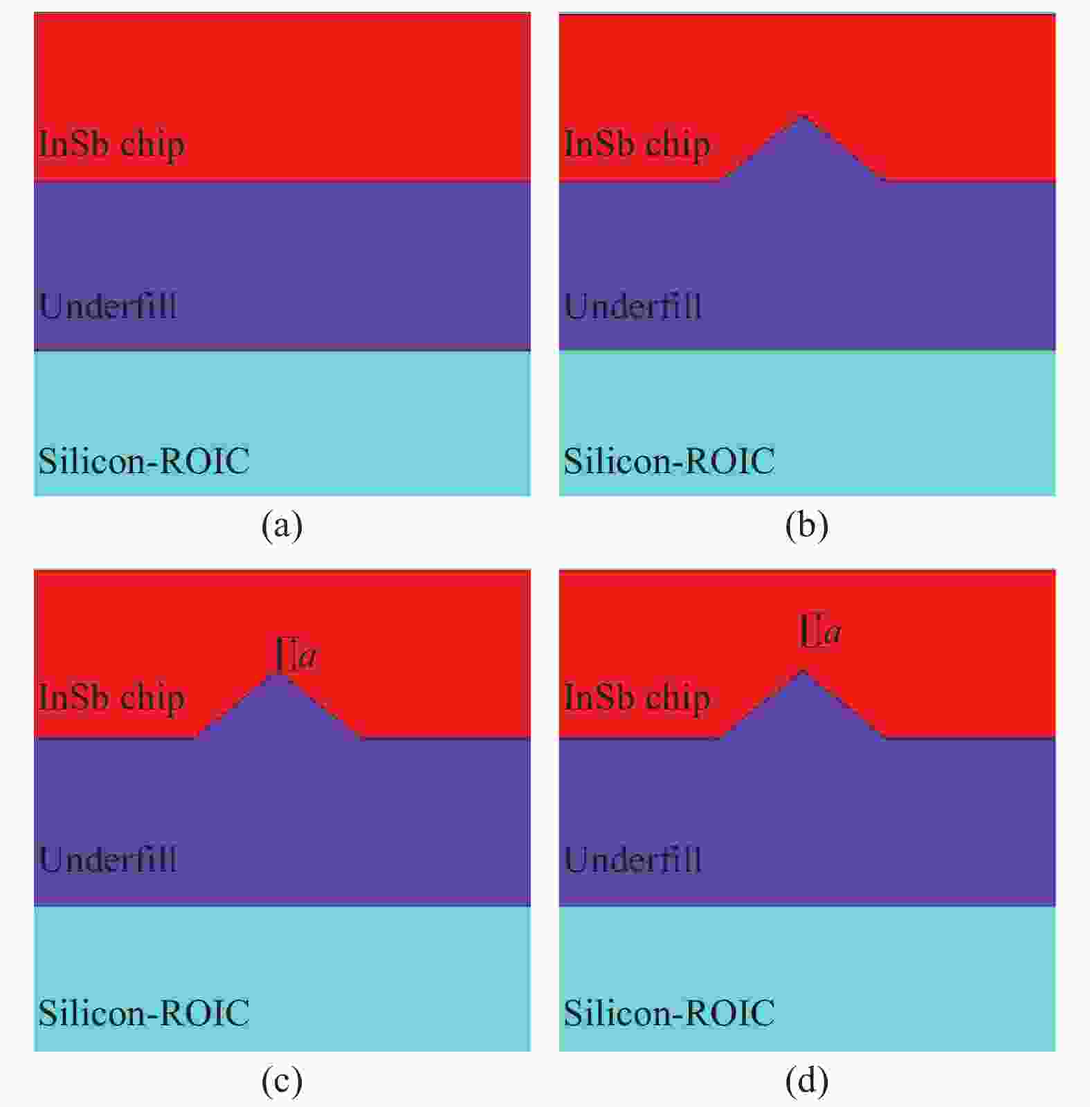
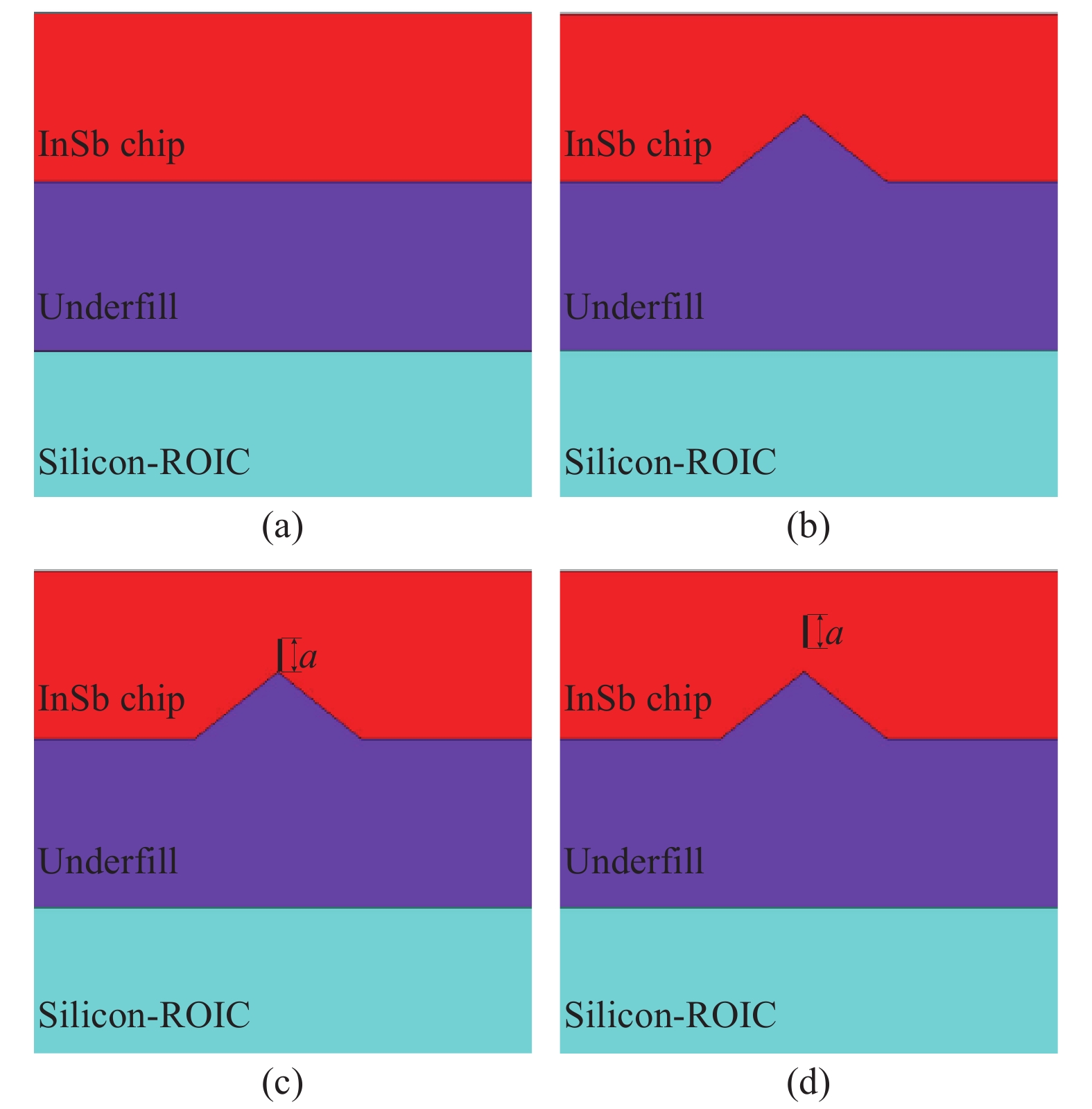
图 1 InSb IRFPAs结构二维模型(局部)。(a) 不包含隔离槽结构的探测器模型;(b) 加入V型隔离槽后的探测器结构模型;(c) 预置裂纹端点和V型槽底部重合的结构模型;(d) 预置裂纹的下端点距V型槽底部为1 μm的结构模型
Figure 1. Two-dimensional model of InSb IRFPAs (local model). (a) Without isolation trough; (b) With V-shaped isolation trough added; (c) Bottom of V-shaped isolation trough is connected with preset crack; (d) Preset crack is away from the bottom of V-shaped isolation trough with a distance of 1 μm
为提高填充因子,InSb 芯片大多采用台面结构形式,此时InSb芯片正面会刻蚀出光敏元隔离槽,即文中的V型隔离槽,填充底充胶后,隔离槽处会充满底充胶。为评估光敏元隔离槽对InSb芯片中累积热应力的影响,给出了不包含隔离槽结构的探测器模型,具体如图1(a)所示;加入V型隔离槽后探测器的结构模型如图1(b)所示,其中V型隔离槽开口宽度为10 μm,槽深4 μm,槽口坐标位于X=3.995 mm到X=4.005 mm的范围内。InSb晶体生长过程中会引入数量不等的位错线,在液氮冲击下,这些位错线可认为是裂纹成核的起源,伴随着热失配应力的增加,位错线会长大、扩展,最终形成穿通裂纹。为了描述隔离槽对InSb芯片中位错线的影响,在V型槽底部预置了不同长度的裂纹,其中预置裂纹下端点和V型槽底部重合的结构模型如图1(c)所示,预置裂纹下端点距V型槽底部为1 μm的结构模型如图1(d)所示。模型中预置裂纹的长度设定为a。
网格划分时,采用自由网格进行单元划分,并对隔离槽处进行加密处理。预置裂纹尖端具有奇异性,裂纹尖端周围的单元是二次奇异单元[14],因此在APDL代码中使用“KSCON”命令对裂纹尖端进行网格化分,第一行单元的半径是裂纹长度的1/10以下,裂纹尖端一圈的单元数量是15。在结构模型的左下角施加固定约束以防止结构移动。
-
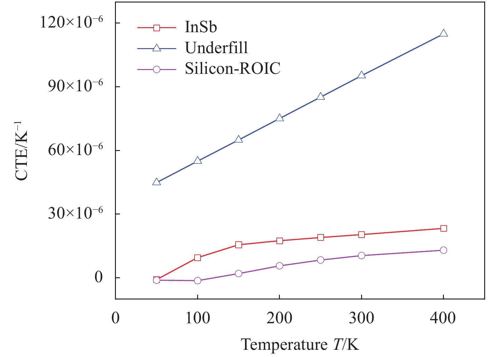
为准确计算InSb IRFPAs中累积的热应变和热应力,材料模型均采用温度相关模型,其中,Silicon-ROIC视为各向同性线弹性材料;忽略底充胶固化过程的底充胶视为线弹性材料;InSb芯片视为各向异性线弹性材料,将InSb芯片的面内杨氏模量值设定为其体积弹性模量值,法线方向的杨氏模量设定为其体积弹性模量的30%,这归因于InSb芯片在背减薄过程中引入的损伤。具体数值如图2和表1所示[15-17],其中E为杨氏模量,v为泊松比。
α为底充胶的线膨胀系数,在77~300 K的温度范围内,可由公式(1)给出:
$$ \alpha {\text{ = 22}}{\text{.46}} \times {\text{1}}{{\text{0}}^{ - 6}} + 5.04 \times {\text{1}}{{\text{0}}^{ - 8}} \times \left( {T - 273} \right) $$ (1) 式中:T的单位为K。

图 2 InSb、底充胶和Silicon-ROIC的线膨胀系数在不同温度下的值
Figure 2. Coefficients of thermal expansion (CTE) depending on temperature for InSb, underfill and Silicon-ROIC
表 1 InSb IRFPAs所用的材料参数和特征尺寸
Table 1. Mechanical parameters and specific sizes of InSb IRFPAs
Materials Elastic modulus E/GPa Poison's ratio v Temperature T/K Length/mm×height/mm InSb 409 (In-plane) 0.35 77-300 10×0.01 123 (Z-direction) Underfill 0.0002/α 0.30 77-300 10×0.01 Silicon-ROIC 163 0.28 77-300 12.8×0.3 -
添加V型隔离槽后的模拟结果如图3所示,这里只给出InSb芯片前表面的面内正应力分布。为便于比对,图3中一同给出不含V型隔离槽时的模拟结果。

图 3 (a) InSb芯片前表面的面内正应力分布;(b) 隔离槽附近区域面内正应力分布
Figure 3. (a) In-plane normal stress distribution of InSb front surface; (b) In-plane normal stress distribution in region of isolation trough existed
对于不含V型隔离槽的结构来说,随着横标远离中心区域,InSb芯片的面内正应力逐渐减小。当V型隔离槽添加后,InSb芯片面内正应力基本维持了这一趋势,但在V型隔离槽存在的区域,面内正应力则发生了较大的变化,即在V型隔离槽的槽底处达到最大值。随着位置偏离槽底,面内正应力急剧变小,在V型槽的开口处减小到最低,并且这一值要低于V型槽添加前的应力值,随着位置继续向V型槽两侧移动,面内正应力逐渐升高,直至与V型槽添加前相同位置处的应力值重叠。
应力分布的定量描述如下:对于不包含隔离槽的结构,当横坐标从由X=0 mm移动到X=5.000 mm时,InSb芯片前表面的面内正应力从505.48 MPa逐渐减小至−369.46 MPa。加入V型隔离槽后,在V型隔离槽开口涵盖区域,即横坐标介于3.995~4.005 mm的范围内,面内正应力由259.65 MPa (X=3.995 mm)降至207.32 MPa (X=3.9958 mm),然后急剧上升至1871.6 MPa (X=4.000 mm处,V型槽的槽底处),紧接着下降至185.19 MPa (X=4.0046 mm),最后上升至262.01 MPa (X=4.005 mm),在隔离槽不存在的区域,二者的差别较小。显然,V型隔离槽加入后会形成应力局部集中,在V型隔离槽槽底处达到最大值。因此InSb芯片最有可能从V型槽槽底起裂。
-
VCCT由Rybicki E F和Kanninen M F提出[18],基于如下的假设,即分离一个表面所需的能量与关闭同一表面所需的能量相同。VCCT的核心是:假设裂纹扩展所释放的能量等于将该裂纹闭合到原始状态所做的功,虚拟裂纹尖端后面的张开位移和实际裂纹尖端后面的张开位移近似相等[11]。对于InSb芯片来说,GC是裂纹扩展所需要的临界能量,表示断裂韧性。根据断裂力学的基本准则,当G>GC,裂纹会扩展。
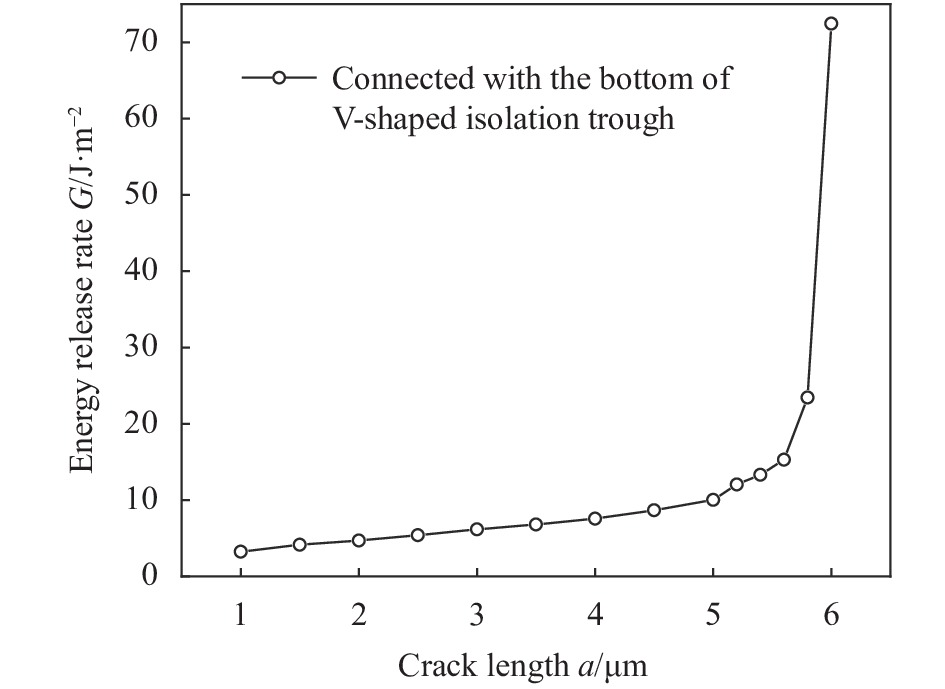
液氮冲击中,裂纹会从InSb芯片位错线处成核并扩展,终止于InSb芯片表面。为此,计算了位错线扩展时的能量释放率,如图4所示。Ⅰ型裂纹的能量释放率(GⅠ)近似等于总能量释放率,Ⅱ型裂纹的能量释放率(GⅡ)接近于零,即G ≈ GⅠ,由此可知,InSb芯片断裂模式是Ⅰ型断裂模式。随着裂纹长度由1 μm增加到5 μm时,能量释放率G由3.2367 J/m2增加至10.047 J/m2,G与a近乎线性关系;当裂纹长度由5 μm增加到6 μm时,裂纹扩展至InSb芯片背面,能量释放率G由10.047 J/m2快速增加至72.455 J/m2,增长速率急剧加大,函数的切线几乎垂直于横轴。因此,当预置裂纹近乎穿透InSb芯片时,能量释放率将会接近一个较大的值,此时,InSb芯片发生断裂的可能性也最大。

图 4 预置裂纹下端点和V型槽底部重合时的能量释放率
Figure 4. Energy release rate of the preset crack connected with the bottom of V-shaped isolation trough
当预置裂纹下端点不与V型槽底重合时,这里假设预置裂纹距离V型槽底的距离为1 μm,在预置裂纹长度分别取1 μm、2 μm、3 μm和4 μm时,模拟得到的裂纹能量释放率如图5所示。显然,在完全相等的预置裂纹长度下,预置裂纹下端点和V型槽底重合时的能量释放率是预置裂纹下端点距V型槽底部1 μm的能量释放率的两倍,表明预置裂纹与V型隔离槽槽底相连通时影响更大,更易引起位错线成核、扩展,形成宏观裂纹。
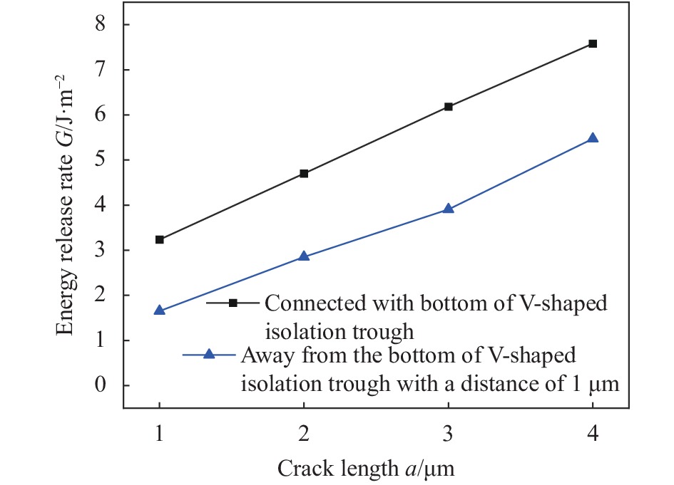
图 5 下端点与V型槽底部重合和下端点距V型槽底部为1 μm的裂纹能量释放率比较
Figure 5. Comparison of energy release rate between the preset crack connected directly with the bottom of V-shaped isolation trough and the preset crack is away from the bottom of V-shaped isolation trough with a distance of 1 μm
-
基于所建的二维有限元模型,分析了光敏元隔离槽对InSb芯片中热应力分布的影响,认为应力集中最易发生在V型隔离槽槽底处,与隔离槽槽底连通的预置裂纹具有更大的能量释放率,更易引起InSb芯片断裂。这为解释液氮冲击中InSb芯片断裂提供了新思路。
Effects of isolation trough on cleavage of InSb chip in InSb detector
-
摘要: 液氮冲击中锑化铟(InSb)芯片的断裂现象制约着InSb红外焦平面探测器(IRFPAs)的成品率。在台面结光敏元阵列中,光敏元之间的隔离槽可能会引起应力集中,驱使InSb芯片中的位错线成核、扩展,导致InSb芯片断裂。为定量分析隔离槽对InSb芯片断裂的影响,建立了InSb IRFPAs结构分析模型,剖析了隔离槽结构的引入对InSb芯片前表面应力分布的影响,发现V型隔离槽槽底是应力集中点;随后在V型隔离槽底预置不同长度的初始裂纹以描述位错线的长短,得到能量释放率随预置裂纹长度之间的关系。经分析后认为:隔离槽确能引起InSb芯片中面内正应力在槽底处产生应力集中;该区域的应力集中有利于InSb芯片中位错线增长,贯穿InSb芯片,导致InSb芯片发生断裂;此外,与V型槽底重合的预置裂纹更易引起InSb芯片发生断裂。这些结论能够为分析InSb芯片的断裂提供新的视角。Abstract: Local cleavage of indium antimonide (InSb) chips restricts the improvement of the yield of InSb infrared focal plane detectors (IRFPAs) under cyclic liquid nitrogen shocking tests. Stress concentration effect may appear in isolation troughs surrounding mesa-junction photosensitive units, drives the dislocation line to nucleate and to propagate, ultimately to punch through InSb chips. In order to analyze quantitatively the influence of isolation troughs on the cleavage of the InSb chip, a structural model of InSb IRFPAs was established, and the in-plane normal stress distribution on the InSb front surface was obtained. Stress concentration phenomena appear on the bottom of V-shaped isolation trough added. Then, the assumed initial cracks with different lengths at the bottom of V-shaped isolation trough were put, here the preset initial cracks were employed to describe dislocation lines in InSb wafers, and were perpendicular to the InSb chips, and obtained the relationship between the energy release rates and the preset crack length. After analyzing these results, the in-plane stress concentration phenomena appears exactly at the bottom of V-shaped isolation trough, and originates from the added V-shaped isolation trough; the enlarged stress at the bottom of V-shaped isolation trough could drive the dislocation lines in the InSb chip to grow and to punch through the InSb chip, thus, the macro cleavage of InSb chip is created; once the preset cracks connect directly with the bottom of V-shaped isolation trough, cleavage of InSb chips is more likely to appear. All these conclusions provide a new perspective to understand the cleavage of InSb chips.
-
Key words:
- InSb detector /
- isolation trough /
- stress /
- energy release rate /
- chip cleavage
-
图 1 InSb IRFPAs结构二维模型(局部)。(a) 不包含隔离槽结构的探测器模型;(b) 加入V型隔离槽后的探测器结构模型;(c) 预置裂纹端点和V型槽底部重合的结构模型;(d) 预置裂纹的下端点距V型槽底部为1 μm的结构模型
Figure 1. Two-dimensional model of InSb IRFPAs (local model). (a) Without isolation trough; (b) With V-shaped isolation trough added; (c) Bottom of V-shaped isolation trough is connected with preset crack; (d) Preset crack is away from the bottom of V-shaped isolation trough with a distance of 1 μm
图 2 InSb、底充胶和Silicon-ROIC的线膨胀系数在不同温度下的值
Figure 2. Coefficients of thermal expansion (CTE) depending on temperature for InSb, underfill and Silicon-ROIC
图 3 (a) InSb芯片前表面的面内正应力分布;(b) 隔离槽附近区域面内正应力分布
Figure 3. (a) In-plane normal stress distribution of InSb front surface; (b) In-plane normal stress distribution in region of isolation trough existed
图 4 预置裂纹下端点和V型槽底部重合时的能量释放率
Figure 4. Energy release rate of the preset crack connected with the bottom of V-shaped isolation trough
图 5 下端点与V型槽底部重合和下端点距V型槽底部为1 μm的裂纹能量释放率比较
Figure 5. Comparison of energy release rate between the preset crack connected directly with the bottom of V-shaped isolation trough and the preset crack is away from the bottom of V-shaped isolation trough with a distance of 1 μm
表 1 InSb IRFPAs所用的材料参数和特征尺寸
Table 1. Mechanical parameters and specific sizes of InSb IRFPAs
Materials Elastic modulus E/GPa Poison's ratio v Temperature T/K Length/mm×height/mm InSb 409 (In-plane) 0.35 77-300 10×0.01 123 (Z-direction) Underfill 0.0002/α 0.30 77-300 10×0.01 Silicon-ROIC 163 0.28 77-300 12.8×0.3  下载: 导出CSV
-
[1] Liu Jiachen, Tang Xin, Ju Yonglin. Numerical simulation on the fast cooling-down process of a miniature infrared detector module [J]. Infrared and Laser Engineering, 2015, 44(3): 816-820. (in Chinese) doi: 10.3969/j.issn.1007-2276.2015.03.005 [2] Bai Wei, Zhao Chao, Liu Ming. Development and application of InSb crystal [J]. Journal of Synthetic Crystals, 2020, 49(12): 2230-2243. (in Chinese) doi: 10.3969/j.issn.1000-985X.2020.12.003 [3] Liang Jinzhi, Xu Changbin, Li Haiyan. Fabrication technology of InSb IR focal plane array [J]. Infrared, 2019, 40(6): 7-12. (in Chinese) doi: 10.3969/j.issn.1672-8785.2019.06.002 [4] Hu Weida, Li Qing, Chen Xiaoshuang, et al. Recent progress on advanced infrared photodetectors [J]. Acta Physica Sinica, 2019, 68(12): 120701. (in Chinese) doi: 10.7498/aps.68.20190281 [5] Bai Wei. Development status of InSb infrared focal plane array detectors [J]. Infrared, 2019, 40(8): 1-14. (in Chinese) doi: 10.3969/j.issn.1672-8785.2019.08.001 [6] Wang Yang, Lu Xing, Meng Chao, et al. Thermal cycle characteristic of InSb focal plane array detector [J]. Infrared and Laser Engineering, 2015, 44(12): 3701-3706. (in Chinese) doi: 10.3969/j.issn.1007-2276.2015.12.034 [7] Lei Shengqiong. Development of InSb infrared material and devices at Kunming Institute of Physics [J]. Infrared and Laser Engineering, 2007, 36(S1): 15-18. (in Chinese) doi: 10.3969/j.issn.1007-2276.2007.z1.007 [8] Wang Wen, Zhang Xiaolei, Lv Yanqiu, et al. InSb infrared focal plane arrays detector based on Si wafer [J]. Infrared and Laser Engineering, 2014, 43(5): 1359-1363. (in Chinese) doi: 10.3969/j.issn.1007-2276.2014.05.001 [9] Mu Hongshan, Dong Suo, Liang Jinzhi. Study of dead pixels in InSb IRFPA detector [J]. Infrared, 2010, 31(7): 9-13. (in Chinese) doi: 10.3969/j.issn.1672-8785.2010.07.002 [10] Meng Qingduan, Zhang Xiaoling, Lv Yanqiu, et al. Function reconsideration of indium bump in InSb IRFPAs [J]. Optical and Quantum Electronics, 2019, 51(9): 304. doi: 10.1007/s11082-019-2021-7 [11] Heidari-Rarani M, Sayedain M. Finite element modeling strategies for 2D and 3D delamination propagation in composite DCB specimens using VCCT, CZM and XFEM approaches [J]. Theoretical and Applied Fracture Mechanics, 2019, 103: 102246. doi: 10.1016/j.tafmec.2019.102246 [12] Geng Hongyan, Zhou Zhou, Song Guofeng, et al. Flip chip bonding technology for IR detectors [J]. Infrared and Laser Engineering, 2014, 43(3): 722-726. (in Chinese) doi: 10.3969/j.issn.1007-2276.2014.03.010 [13] Yang D G, Ernst L J, van`t Hof C, et al. Vertical die crack stresses of flip chip induced in major package assembly processes [J]. Microelectronics Reliability, 2000, 40(8-10): 1533-1538. doi: 10.1016/S0026-2714(00)00156-6 [14] Wang L, Yang J S, Ni J X, et al. Influence of cracks in APS-TBCs on stress around TGO during thermal cycling: A numerical simulation study [J]. Surface & Coatings Technology, 2016, 285: 98-112. [15] He Y, Moreira B E, Overson A, et al. Thermal characterization of an epoxy-based underfill material for flip chip packaging [J]. Thermochimica Acta, 2000, 357-358: 1-8. doi: 10.1016/S0040-6031(00)00357-9 [16] Meng Qingduan, Zhang Xiaoling, Zhang Liwen, et al. Structural modeling of 128× 128 InSb focal plane array detector [J]. Acta Physica Sinica, 2012, 61(19): 190701. (in Chinese) doi: 10.7498/aps.61.190701 [17] Meng Qingduan, Yu Qian, Zhang Liwen, et al. Mechanical parameters selection in InSb focal plane array detector normal direction [J]. Acta Physica Sinica, 2012, 61(22): 226103. (in Chinese) doi: 10.7498/aps.61.226103 [18] Rybicki E F, Kanninen M F. A finite element calculation of stress intensity factors by a modified crack closure integral [J]. Engineering Fracture Mechanics, 1977, 9: 931-938. doi: 10.1016/0013-7944(77)90013-3 -

 点击查看大图
计量
- 文章访问数: 202
- HTML全文浏览量: 48
- PDF下载量: 40
- 被引次数: 0