


-
红外滤光片是一种广泛应用于遥感探测、气体分析、安防监测、气象预报和自动驾驶等领域的光谱滤波元件,它可以精确提取探测所需要的波段,并对工作波段以外的辐射能量进行抑制[1-3]。在红外空间遥感领域,根据大气窗口通常将波段划分为短波红外(1~3 μm)、中波红外(3~5 μm)和长波红外(8~14 μm)[4]。随着红外背景干扰因素的增多,单波段探测在抗干扰方面存在一定的困难,而红外双波段探测技术因其可以同时获得两个光谱通道内的信息、具备分辨能力高、抗干扰能力强等优点,是红外探测技术发展的方向之一[5-7]。两个光谱通道的信息配合双色探测器,可以得到两个光谱通道的差分信息、合成信息和分别的单独信息,使得探测的准确性明显提升。
不同于在一个元件上分区域镀膜实现两个光谱通道探测,双带通滤光片可以在一个元件的任意几何位置通过多层薄膜干涉同时形成两个光谱通道,并且抑制光谱通道以外的辐射能量。红外双带通滤光片可以提升工作通道内的光学效率,减少光学系统的复杂度,还能避免光谱通道间的杂光串扰问题。
相比传统的单带通滤光片,双带通滤光片在设计时需要同时平衡两个通道的光谱形状和两个通道之外的光谱抑制,在膜层制备时需要对多个敏感层实现1%以内的高精度控制。陈友华等[8]选用PbTe和ZnSe作为高低折射率膜层材料,设计了一种具有5.9~6.2 μm和11.9~12.2 μm的双带通滤光片,两个光谱通道的透过率分别达到90%和65%;Brian T. Sullivan等[9]在波长400~600 nm的可见光范围内采用全非规整膜系研制了一种双带通滤光片,两个通带的中心波长分别为468 nm和532 nm,带宽均为10 nm;蔡渊等[10]提出了一种兼有增透带的Fabre-Perot (F-P) 膜系组合设计的方法,有效解决了通道间光谱距离较大时双色滤光片的设计难题;陈旭等[11]采用多个截止带组合的设计方法,选用Si和SiO膜层制备了一种中心波长分别为3.0 μm和4.5 μm的双通道滤光片,两个通道的透射率分别达到73%和81%,该方法对于传统设计的继承性好,但制作时通带光谱的控制较难。
文中研制了一种在100 K低温环境下使用的短波和中波红外双带通滤光片。利用滤光片基片的两个表面,其上各制作一个兼有特定增透波段(另一面上的F-P带通波段) 的F-P带通滤光膜系。当光线穿过滤光片时,两个设计的F-P带通部分能够高效率地透射,而其他波长的光线则被有效拦截,实现双带通的效果。这样做的好处是可以准确设计和镀制得到单个F-P带通的光谱,对另一个带通的影响较小,有利于得到好的光谱品质和成功率。设计时,考虑了常温300 K和低温100 K情况下膜层和基片的光学特性的差异,研究了双带通滤光片在常温和低温条件下的光谱变化情况。
-
双带通滤光片的膜系设计通常有两种方法[12]:第一种是通过负滤光膜系和宽带通膜系叠加的方式形成双带通滤光膜系;第二种是基于两个兼有特定增透带的F-P单带通滤光膜系,叠加形成双带通滤光膜系。这样的叠加通常设置在基片的两个表面上,可以避免膜系之间的干扰。文中设计的双带通滤光片的短波通道(2.60~2.85 μm)和中波通道(4.10~4.40 μm)分别位于短波红外和中波红外区域,通道之间相隔较远,而且每个通道都有独立要求的中心波长和带宽,因此选择第二种方法进行膜系设计。
短波和中波红外滤光片常用的基片有Ge、Si、ZnSe和蓝宝石,其光学和力学性能如表1所示[13]。
表 1 Ge、Si、ZnSe和蓝宝石的光学和力学性能
Table 1. Optical and mechanical properties of Ge, Si, ZnSe and sapphire
Refractive
indexTransparent
wavelength/
μmYoung's
modulus/
N·m−2Linear expansion
coefficient/
℃Ge 4.0 2.0–12.5 10.3×10¹⁰ 5.5×10⁻⁶ Si 3.4 1.4–8.0 13.1×10¹⁰ 4.2×10⁻⁶ ZnSe 2.4 0.8–14.0 5.4×10¹⁰ 7.1×10⁻⁶ Sapphire 1.75 0.2–5.0 34.5×10¹⁰ 6.7×10⁻⁶ 从表1可以看出,在这些材料中,蓝宝石基片在2.6~4.4 μm区间有良好的透明性,其线膨胀系数与膜层材料Ge相近,适合在低温条件下使用。因为在高温(250 ℃左右)条件下镀制的滤光片需要在低温(100 K)下工作,温度变化达到420 ℃之多。
膜层材料选用Ge和SiO,它们在工作通道内都有良好的光学透明性。在滤光片基片的前表面设计了2.60~2.85 μm单带通滤光膜系,同时设计保持了4.0~4.5 μm波段高透过性能;在基片的另一个表面设计4.10~4.40 μm的单带通滤光膜系,同时设计保持了2.5~2.9 μm波段的高透射性能。通过基片前后表面膜系的组合,叠加形成双带通滤光效果。
-
红外双带通滤光片的工作温度为100 K,为了使滤光片在低温下具有良好的光学性能,需要采用100 K温度下膜层的光学参数进行膜系设计。
通过测量Ge和SiO单层薄膜在常温和低温下的透射光谱,再利用Cauchy模型对其拟合,得到Ge和SiO在常温和低温下的折射率值[14-15]。Ge薄膜沉积采用电子束蒸发的方式,电子枪高压为8 kV,束流为200 mA。SiO薄膜沉积采用电阻热蒸发的方式,阻蒸电压为10 V,电流为550 A。Ge和SiO单层膜沉积在ZnSe基片上,其透明光谱区域为1~20 μm。Ge和SiO膜层的制备工艺参数如表2所示(1 Å=0.1 nm)。
表 2 Ge和SiO膜层的制备工艺参数
Table 2. Preparation parameters of Ge and SiO layers
Substrate temperature/
℃Evaporation rate/
Å·s−1Vacuum pressure/
10−4 PaGe film 250±5 6±2 6–8 SiO film 250±5 15±3 6–8 薄膜样品的低温光谱测试在Perkin-Elmer公司制造的Spectrum GX型傅里叶红外光谱仪上进行。测量时将样品台放入低温杜瓦中,样品保持在真空环境中。样品在液氮和加热器的共同作用下实现温度调节,温控精度达到±0.3 K。测量时扣除了背景影响。
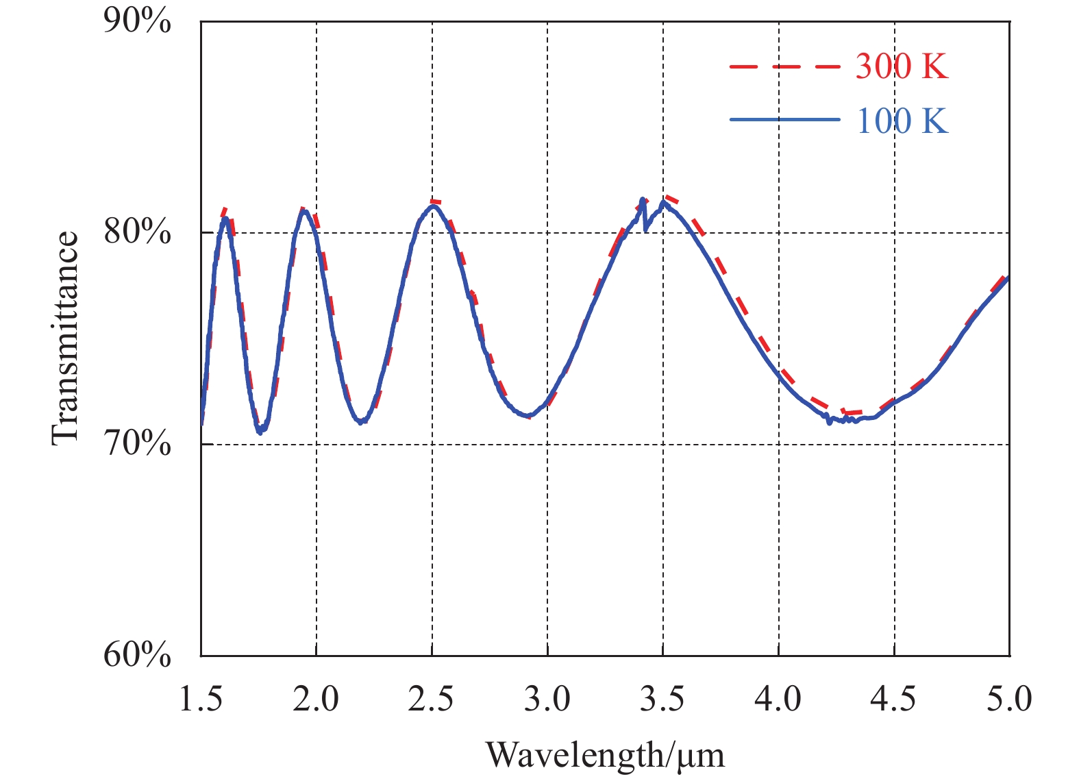
图1和图2为Ge薄膜和SiO薄膜在300 K和100 K温度下的透射光谱曲线。

图 1 Ge薄膜在300 K和100 K温度下的透射光谱
Figure 1. Transmission spectrum of Ge single layer film at 300 K and 100 K temperature

图 2 SiO薄膜在300 K和100 K温度下的透射光谱
Figure 2. Transmission spectrum of SiO single layer film at 300 K and 100 K temperature
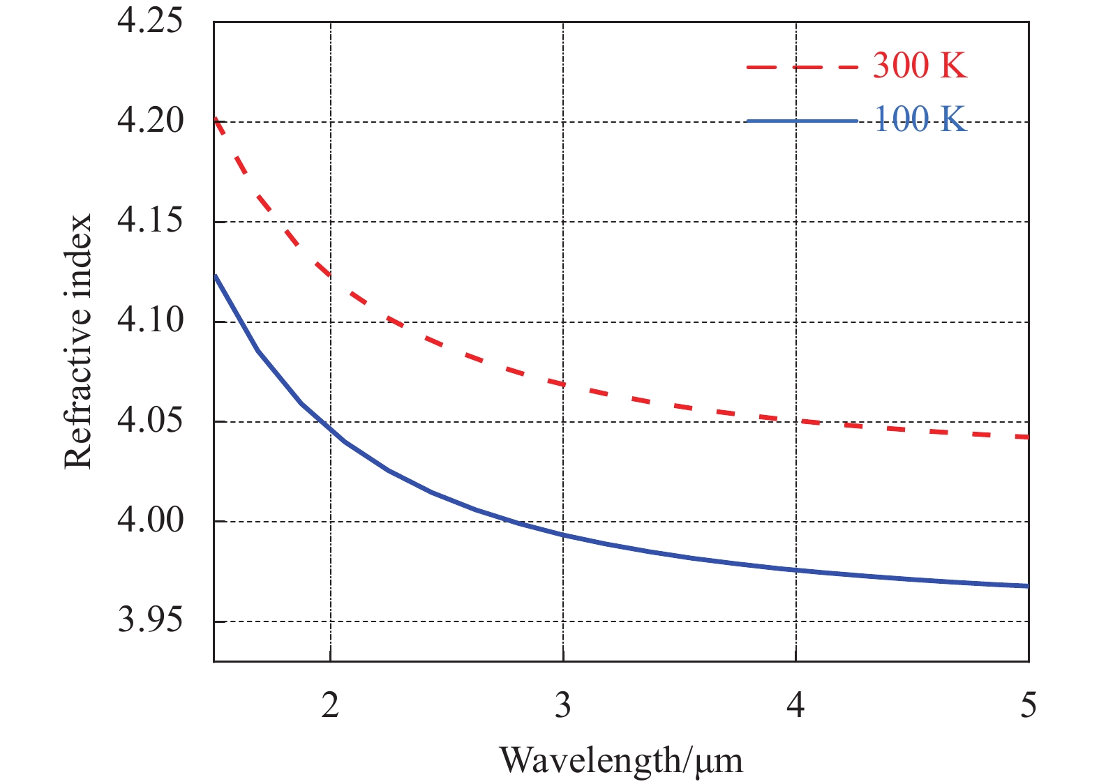
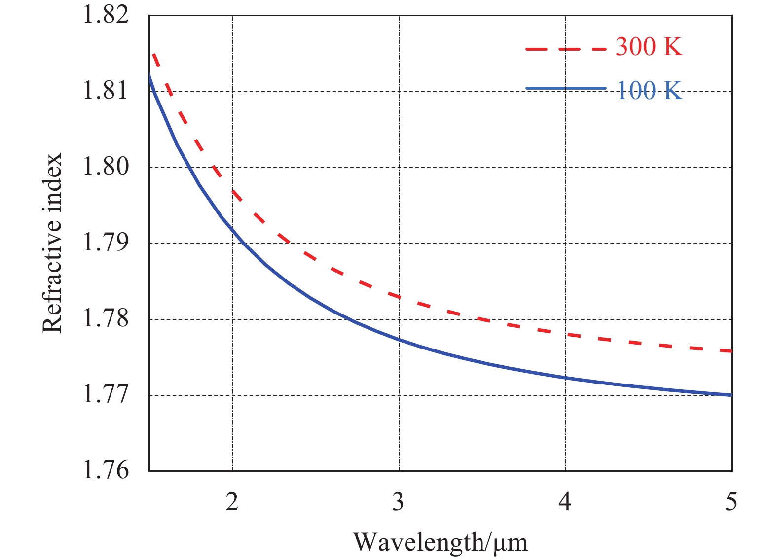
使用FilmWizard软件对Ge和SiO单层膜的透射光谱进行了拟合,得到了它们在300 K和100 K温度下的折射率光谱曲线,分别如图3和图4所示。

图 3 Ge薄膜在300 K和100 K温度下的折射率拟合曲线
Figure 3. Refractive index fitting curves of Ge single layer film at 300 K and 100 K temperature

图 4 SiO薄膜在300 K和100 K温度下的折射率拟合曲线
Figure 4. Refractive index fitting curves of SiO single layer film at 300 K and 100 K temperature
-
F-P 膜系的结构为:[反射层│间隔层│反射层]k,主要有以下两种形式[16]:
$$ [\cdots{\rm{LHL}}\left|{\rm{mH}}\right|{\rm{LHL}} \cdots]^{k} 或 [\cdots {\rm{HLH}}\left|{\rm{mL}}\right|{\rm{HLH}}\cdots]^{k} $$ 式中:H代表高折射率膜层;L代表低折射率膜层;k为正整数;m是不小于2的偶数。通带宽度可表示为:
$2\Delta \lambda = \dfrac{{4{\lambda _0}n_{\rm{L}}^{2 x - 1}{n_{\rm{g}}}}}{{m\pi n_{\rm{H}}^{2 x}}} \cdot \dfrac{{{n_{\rm{H}}} - {n_{\rm{L}}}}}{{{n_{\rm{H}}} - {n_{\rm{L}}} + {{{n_{\rm{L}}}} \mathord{\left/ {\vphantom {{{n_{\rm{L}}}} m}} \right. } m}}}$ (H作为间隔层)或
$2\Delta \lambda = \dfrac{{4{\lambda _0}n_{\rm{L}}^{2 x}{n_{\rm{g}}}}}{{m\pi n_{\rm{H}}^{2 x + 1}}}\cdot \dfrac{{{n_{\rm{H}}} - {n_{\rm{L}}}}}{{{n_{\rm{H}}} - {n_{\rm{L}}} + {{{n_{\rm{L}}}} \mathord{\left/ {\vphantom {{{n_{\rm{L}}}} m}} \right. } m}}}$ (L作为间隔层)式中:nH和nL分别为高低折射率膜层的折射率;ng为基片折射率;x为反射膜内高折射率膜层数;m为谐振腔干涉级次,它与间隔层厚度的关系为:m=2 nd/λ0。
根据滤光片的带宽要求,将初始膜系确定为:
Sub. // LHL 2 H LHL 4 H LHL 4 H LHL 2 H LHL // Air
对应的设计波长为2.725 μm。经过对通道内的顶部波纹的优化,单带通滤光片的设计光谱如图5所示。
图 5 短波通道滤光膜系的设计光谱
Figure 5. Designed transmittance curve of the short-wavelength band-pass filter
可以看到,滤光片的带宽为262 nm,已经在设计要求的公差范围之内,但还无法使4.10~4.40 μm波段内的光波实现透射。为此,采用了Needle优化算法进行辅助设计:将单带通滤光片的膜系结构作为初始膜系,优化目标值同时设置了通带 (2.60~2.85 μm和4.05~4.45 μm) 内的高透射和通道外(2.00~2.50 μm 和3.00~3.60 μm)的深截止,通过自动添加适当数量的膜层和全局优化,使优化后膜系的透射光谱性能够达到或接近设计要求。优化后的膜系结构如下:
Sub. // 1.190 L 0.200 H 4.531 L 0.689 H 0.819 L 2.410 H 0.434 L ···(8 layers)···2.279 H 0.706 L 0.837 H 1.017 L 2.561 H 0.441 L 0.377 H 0.526 L // Air
优化后的透射光谱如图6所示。
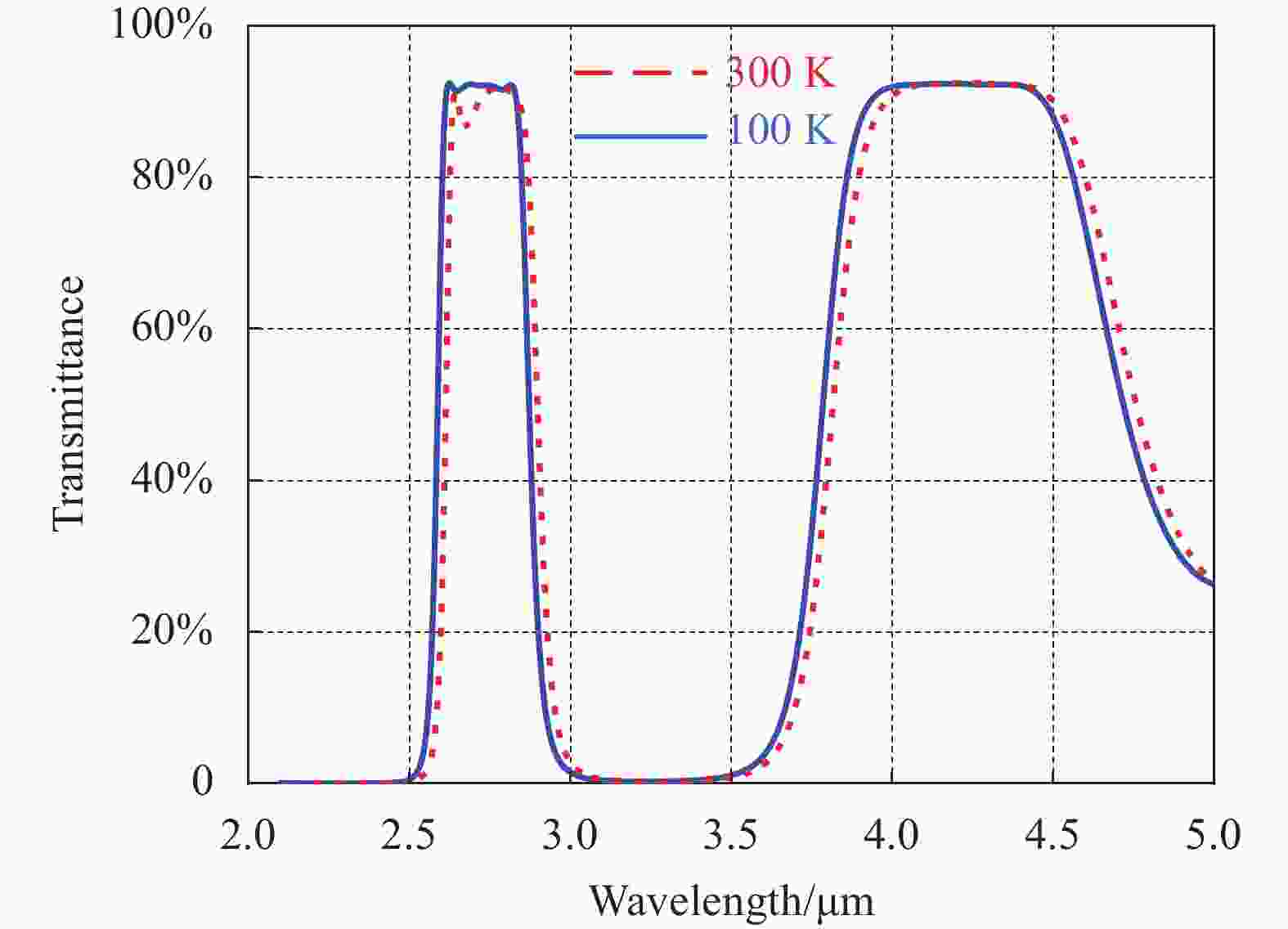
图 6 短波通道滤光膜在100 K和300 K温度下的设计光谱
Figure 6. Designed transmittance curve of the short-wavelength band-pass filter with transmitted longer band at 100 K and 300 K temperature
从设计光谱可以看到,短波通道滤光膜系的低温光谱较常温光谱向短波方向移动,光谱形状发生明显变化。这是由于在膜系设计时,分别采用了Ge和SiO膜层在100 K和300 K温度下的折射率值,如表3所示。
表 3 Ge和SiO单层膜在300 K和100 K温度下的折射率
Table 3. Refractive index of Ge and SiO single layer film at 300 K and 100 K temperature
300 K 100 K Ge film 4.05 3.97 SiO film 1.78 1.77 在100 K温度下,膜层的折射率值和光学厚度减小,滤光片的光谱也向短波方向偏移[17]。光谱的偏移量可以通过计算和测量得到,并且具有确定性。在制备滤光片时,根据实际工作温度向长波方向预设偏移量。
滤光膜系的光谱形状因温度改变也发生了明显的变化。因为滤光片在设计时采用了低温(100 K)下的光学参数,在低温下能够接近理想光谱,而在常温下通带的光学匹配不够充分。短波滤光膜系采用了非规整膜层进行设计,各个间隔层的厚度不相等,在折射率随温度改变的过程中,膜层光学厚度的减小量是不相等的,这也增加了通带光谱形状随温度变化的改变量。F-P膜系的间隔层的光学厚度对其光谱的影响明显,图7为短波通道滤光膜系的间隔层光学厚度分别改变1%、2%和3%情况下的透射光谱。

图 7 短波通道滤光膜系在间隔层光学厚度分别增加1%、2%和3%情况下的透射光谱
Figure 7. Transmission spectrum of the shorter band-pass filter film when the optical thickness of the spacer layers are increased by 1%, 2% and 3%, respectively
表4列出了短波通道滤光膜系在100 K和300 K温度时的平均透射率Tave、顶部波纹振幅(
$\Delta $ =Tmax−Tmin)和两侧边缘陡度(g =∣λ0.8−λ0.1∣/λ0.5)的设计值。可以看到,短波通道滤光膜系在100 K工作温度时比在300 K温度时具有更好的光学性能。表 4 短波通道滤光膜系在100 K和300 K温度下的设计光学性能
Table 4. Designed optical properties the shorter band-pass filter film at 100 K and 300 K temperature
100 K 300 K Average transmittance Tave 92.0% 89.9% Ripple amplitudes $\Delta $ 1.1% 5.5% Left edge steepness gL 1.1% 1.2% Right edge steepness gR 1.8% 2.0% 由于采用了膜层在实际工作温度(100 K)下的折射率值进行膜系设计,低温下具有更好的光谱性能,也更符合应用需求。
-
中波通道(4.10~4.40 μm)滤光膜系的设计思想与短波通道的相同,基于F-P单通道膜系结构,通过优化膜系,保证4.10~4.40 μm通带波形良好的同时,使得2.5~2.9 μm波段也能够高透过。根据滤光片的带宽要求,初始膜系确定为:
Sub. // HLH 4 L HLH 4 L HLH 4 L HLH 4 L HL // Air
采用Needle优化算法通过TFCalc软件进行辅助设计,同时设置了两个优化目标值:通带内(2.5~2.9 μm和4.10~4.40 μm)的高透射和通道外(4.60~5.00 μm 和3.50~3.90 μm)的高截止,再通过自动添加适当数量的膜层和全局优化,使优化后膜系的光谱性能符合设计要求。优化后的膜系结构如下:
Sub. // 0.062 H 0.406 L 1.306 H 3.773 L 1.175 H 1.108 L ···(8 layers)··· 0.852 H 1.127 L 0.977 H 3.851 L 1.156 H 0.557 L // Air
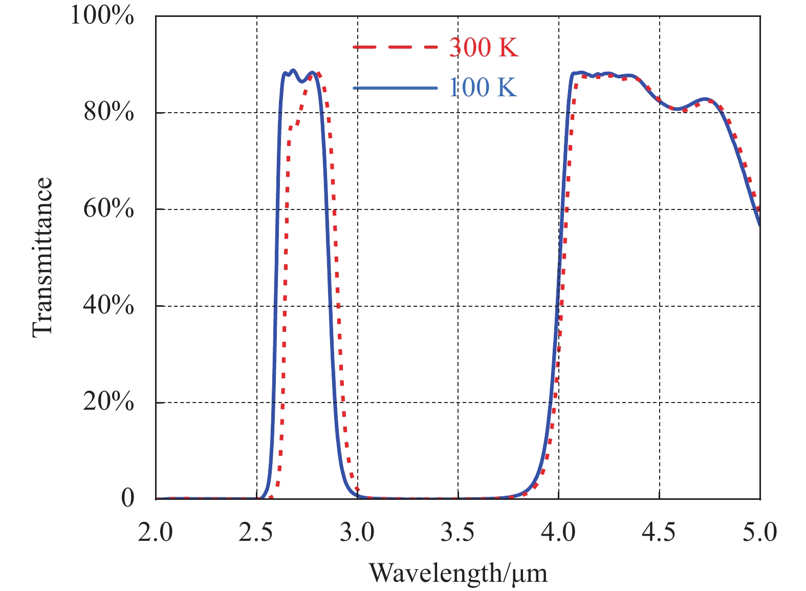
中波通道滤光膜系的设计光谱如图8所示。

图 8 中波通道滤光膜在100 K和300 K温度下的设计光谱
Figure 8. Transmittance curves of the designed middle-wavelength band-pass filter with transmitted shorter band at 100 K and 300 K temperature
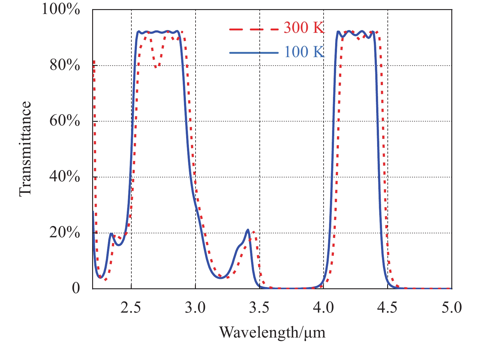
分别位于两个表面上的短波通道滤光膜系和中波通道滤光膜系,叠加组合后综合得到了完整的双带通滤光膜系,这一完整膜系在300 K和100 K工作温度下的透射光谱设计曲线如图9所示。

图 9 双带通滤光片在100 K和300 K温度下的设计光谱
Figure 9. Designed spectrum of the dual band-pass filter at 100 K and 300 K temperature
可以看出,这样的设计光谱能够达到预期目标,在两个工作光谱通道处实现了高透射的通带,在其他光谱波段实现了良好的截止。
-
Ge和SiO膜层镀制分别采用电子束和电阻热蒸发的方式,膜厚控制采用光学监控方式。膜层沉积前用射频离子源对蓝宝石基片表面进行了清洁和激活处理。膜层沉积过程中,基片温度保持在(250±10) ℃范围内。
优化后膜系中的敏感层比较多,对膜厚的控制精度要求较高,采用原位透射测量的方式较好地实现了对膜层厚度的精确监控。监控曲线采用MCalc软件进行了预先设计,结合单波长光学极值百分比(POEM)监控策略,使得监控过程具有自补偿能力。当某一层膜的光学厚度出现监控误差时,下一层膜在镀制时能够得到部分补偿,适合F-P滤光膜系的膜厚监控。
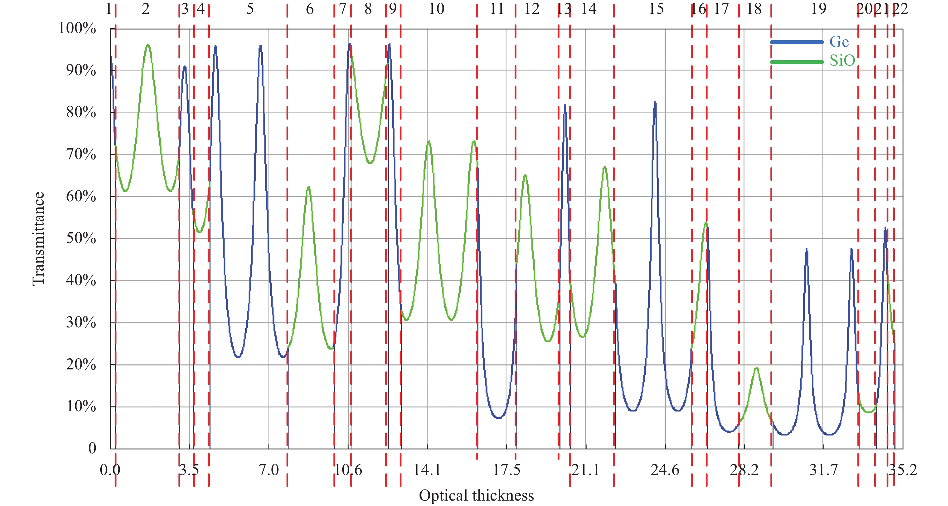
图10给出了短波滤光膜系的预设监控曲线,监控波长选用2 020 nm。图中蓝色和绿色曲线分别表示在2 020 nm的监控波长下,Ge和SiO膜层的透射率随光学厚度增加的变化情况。为保证每一层膜厚可以被精确监控,在监控波长选择时,尽可能使监控停止位距离下一个极值点保持4%*(Tmax−Tmin)以上距离。中波通道滤光膜系的制备和监控方法与此类似。

图 10 短波通道滤光膜系2 020 nm的单波长POEM预设监控曲线
Figure 10. Simulated monitor curve of single-wavelength POEM at 2 020 nm for the shorter band-pass filter film
-
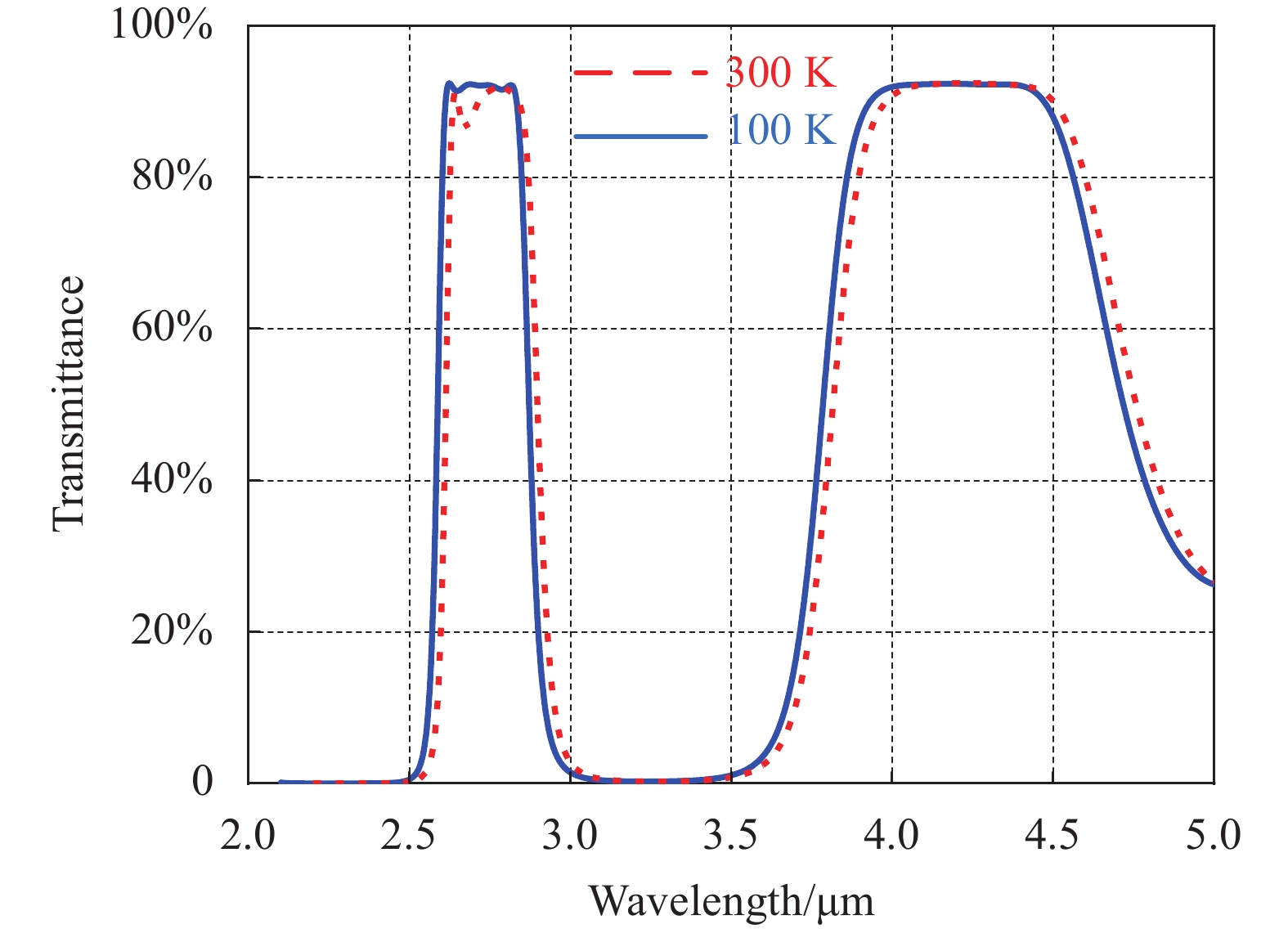
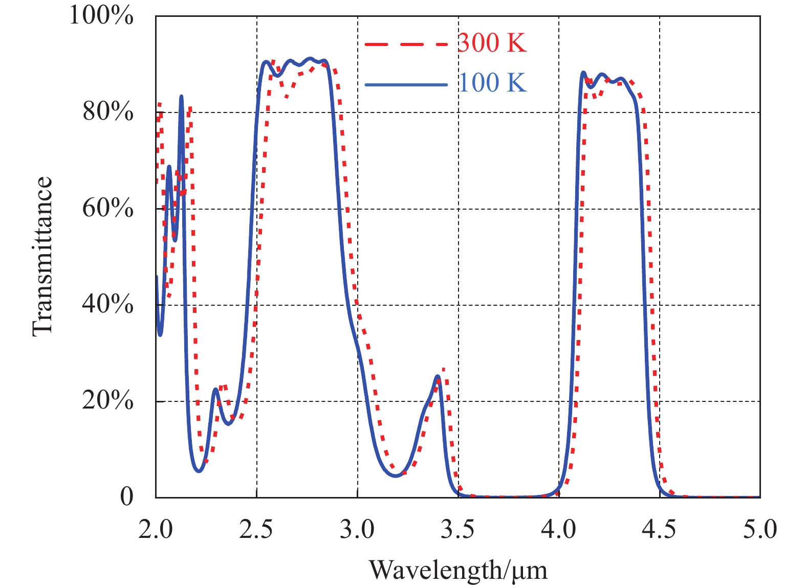
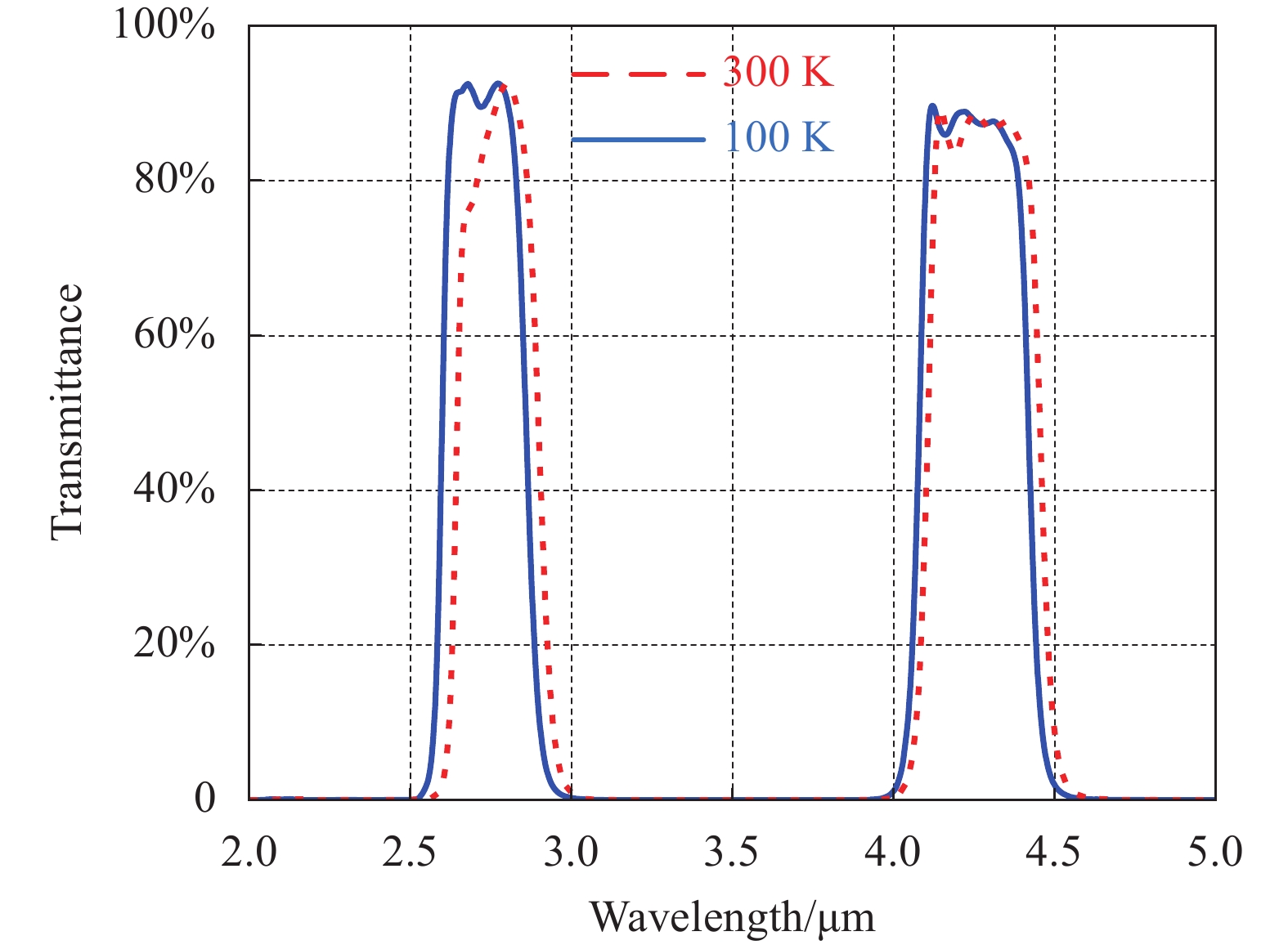
在300 K和100 K温度下分别测量了短波通道滤光膜系、中波通道滤光膜系和合成后双带通滤光膜片的透射光谱,测量方法与测量Ge和SiO单层薄膜透射光谱的方法相同。测量结果分别如图11、图12和图13所示。
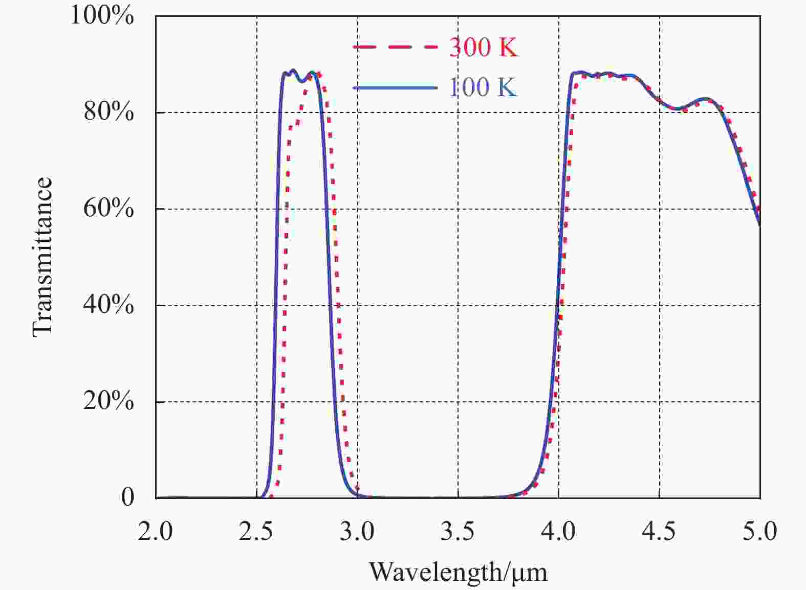
图 11 短波通道滤光膜系在100 K和300 K温度下的透射光谱测量曲线
Figure 11. Measured transmittance spectra curves of the short-wavelength band-pass filter film at 100 K and 300 K temperature
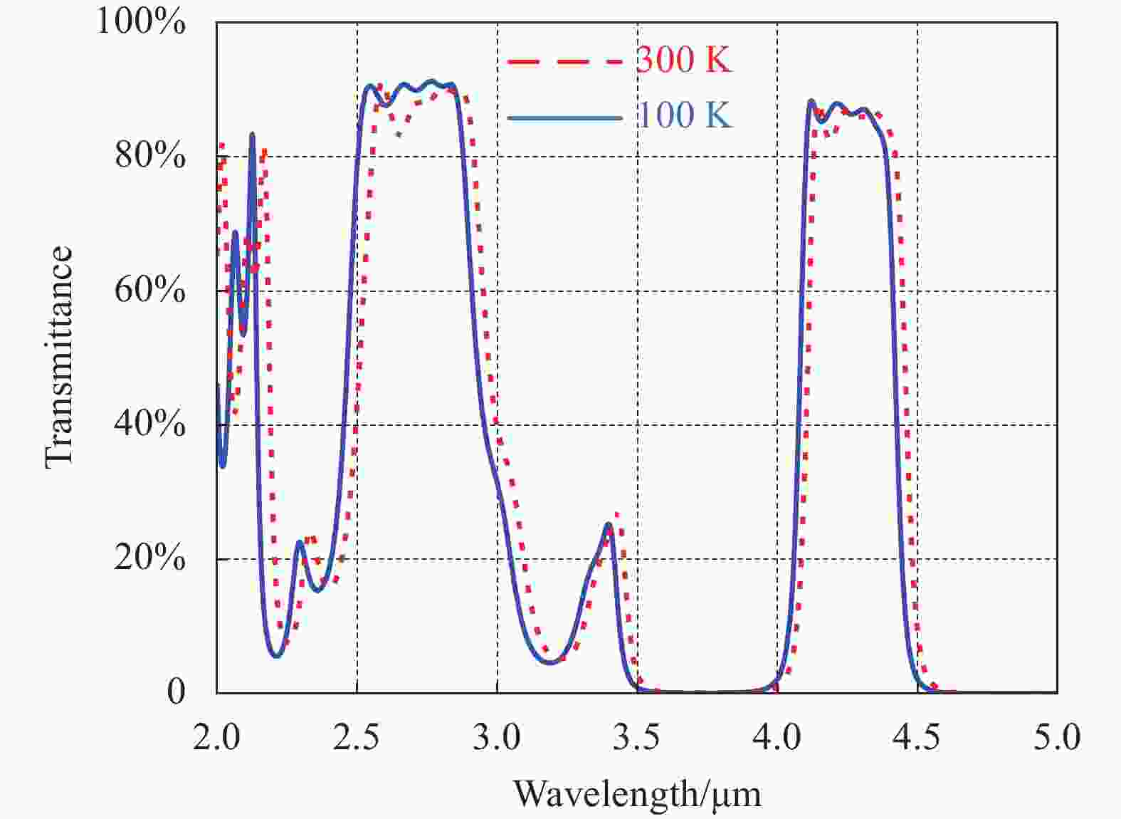
图 12 中波通道滤光膜系在100 K和300 K温度下的透射光谱测量曲线
Figure 12. Measured transmittance spectra curves of the middle-wavelength band-pass filter film at 100 K and 300 K temperature
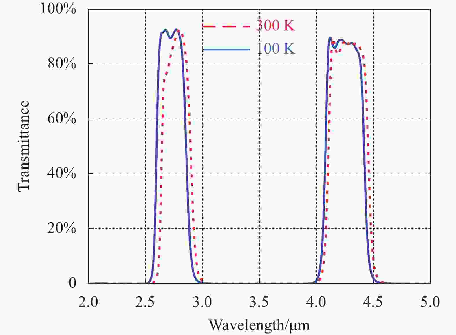
图 13 双带通滤光片在100 K和300 K温度下的透射光谱测量曲线
Figure 13. Measured spectra transmittance curves of the dual band-pass filter at 100 K and 300 K temperature
低温透射光谱测量结果显示,双带通滤光片在工作温度下,两个通道都具有良好的光学性能。其中短波通道(2.60~2.85 μm)和中波通道(4.10~4.40 μm)的平均透射率分别为91.2%和87.7%,短波和中波通道之间(3.00~3.95 μm)的截止区域平均透过率小于0.1%。两个通道的顶部波纹振幅和边缘陡度的数值如表5所示。
表 5 短波和中波通道的顶部波纹幅度和边缘陡度
Table 5. Top ripple amplitudes and edge steepness of the shorter and the longer channel
Top ripple amplitude Left edge steepness Right edge steepness Short-wavelength channel
(2.60-2.85 μm)2.1% 1.6% 2.3% Middle-wavelength channel
(4.10-4.40 μm)3.8% 1.3% 1.4% 伴随着温度降低,双带通滤光片的透射光谱向短波方向移动。表6列出了短波和中波通道两侧半功率点的波长位置在降温过程中的偏移量。
表 6 300~100 K降温过程中短波和中波通道的半功率点的偏移量
Table 6. T0.5P position shift value of the shorter and the longer channels while temperature reduces from 300 K to 100 K
Left T0.5P position shift value Right T0.5P position
shift value/nmShort-wavelength channel
(2.60-2.85 μm)−48 −40 Middle-wavelength channel
(4.10-4.40 μm)−29 −36 从测试结果可以看出,双带通滤光片的透射率和顶部波纹幅度略差于设计效果,主要原因是:薄膜制备过程中存在一定的厚度控制误差,双带通滤光膜系又比较复杂,敏感层较多,各层膜厚误差累积后使得顶部波纹的幅度变大,透过率也有所降低。
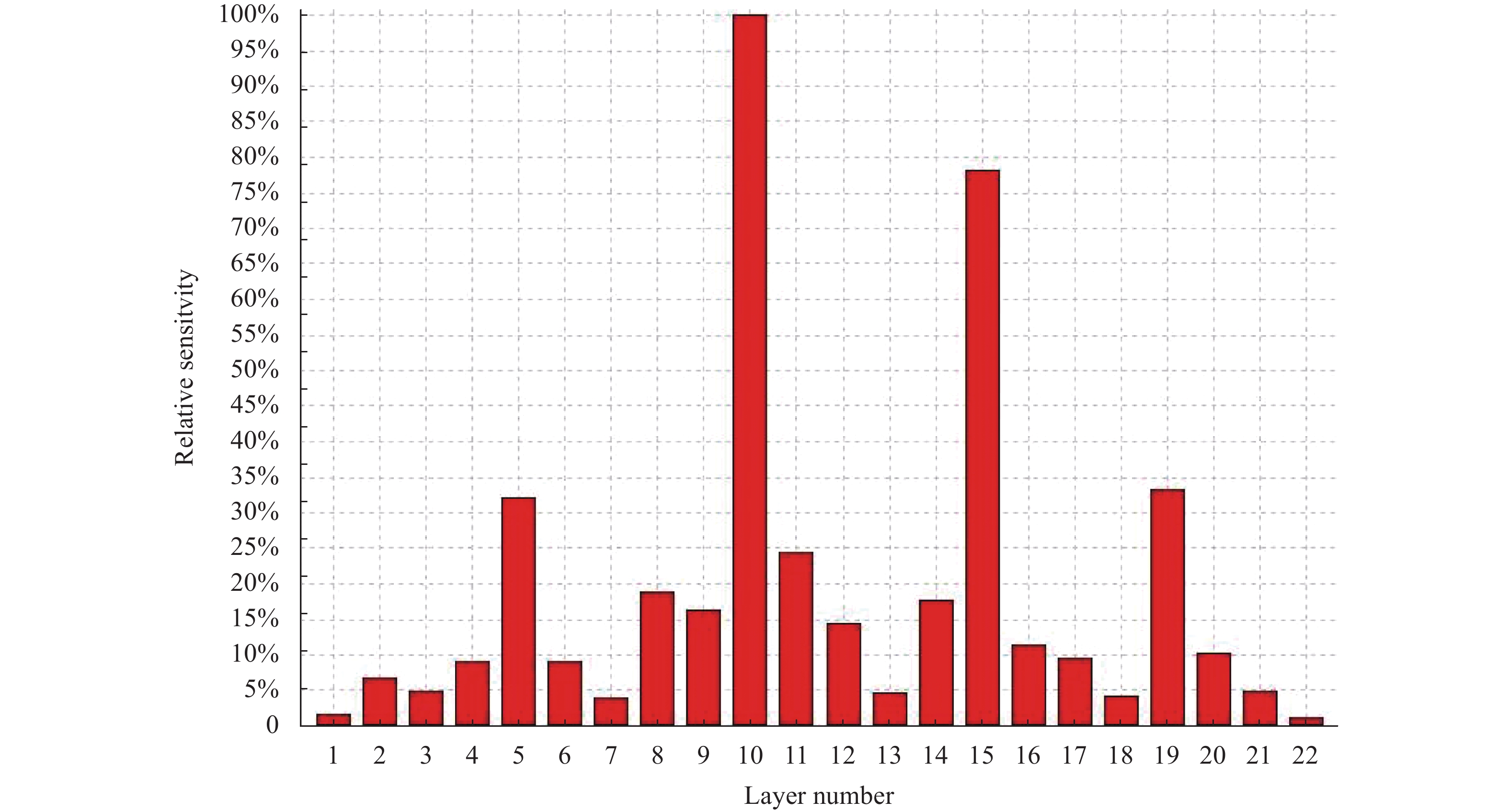
图14中,利用OptiLayer薄膜设计软件对短波通道滤光膜系进行了膜层误差引起光谱变化的灵敏度分析。可以看出,膜系的第5、10、15和19层的灵敏度较大,这几层都是膜系中的间隔层(谐振腔层)。可见,特别需要对间隔层的光学膜厚进行精确控制。

图 14 短波通道滤光膜系中各膜层的灵敏度
Figure 14. Sensitivity of each layer in the shorter band-pass filter
对短波通道滤光膜系中最敏感的第5、10、15和19层引入1%~3%的随机误差,观察这样的误差对透射率光谱曲线的影响。引入误差后的透射率曲线如图15所示。可以看出,引入误差对4.10~4.40 μm透射区的影响很小,但对2.60~2.85 μm通道的光谱形状有较大影响。超过1%的随机误差就会使短波通道的透射性能明显下降。在膜层实际制备过程中,通过原位透射监控方式并结合单波长光学极值百分比(POEM)监控策略后,将间隔层的厚度误差控制在1%以内,得到了透射性能良好的双带通滤光片。

图 15 短波通道滤光膜系的第5、10、15和19层引入1%~3%的随机误差后的透射光谱曲线
Figure 15. Transmission spectrum curves of the shorter band-pass filter film when random errors of 1%-3% introduced into the 5th, 10th, 15th and 19th layers
-
以蓝宝石(Al2O3)为基片,用Ge和SiO作为高低折射率膜层,设计制备了兼有增透带的Fabre-Perot 结构带通滤光膜系:短波通道滤光膜系和中波通道滤光膜系,它们分别位于基片的两个表面,这两个膜系叠加合成了双带通滤光片。设计时,膜层的光学常数选用了100 K低温条件下的测量数值。得到的低温滤光片包含短波通道(2.60~2.85 μm)和中波通道(4.10~4.40 μm),低温下的波形和透射光谱性能比常温下更好。Ge和SiO膜层分别以电子束和电阻热蒸发方式在高真空环境中完成沉积。测量了300 K和100 K温度下双带通滤光片的透射光谱。结果显示:由于低温下膜层折射率降低,相当于膜层的光学厚度减少,使得滤光片的透射光谱向短波方向移动,漂移量在29~48 nm范围。短波和中波通道的平均透射率分别达到91.2%和87.7%,顶部波纹幅度分别控制在2.1%和3.8%以内,波长3.00~3.95 μm光谱区域内的截止深度达到0.1%。这样的红外双带通滤光片在低温下工作时有更好的光谱,有利于更加精确的红外遥感和探测。
Design and fabrication of short and middle wavelength infrared dual band-pass filter at cryogenic temperature
-
摘要: 双带通滤光片可以在元件的任意一个几何位置上同时透过两个光谱通道,从而实现双光谱通道的同时探测。文中研制了一种在100 K低温下使用的短波和中波红外双带通滤光片,选用Ge和SiO分别作为高低折射率膜层,在蓝宝石(Al2O3)基片上设计了具有Fabre-Perot(F-P)结构的短波通道滤光膜系和中波通道滤光膜系,它们在另一通带位置兼具增透能力,组合形成了包含短波通道(2.60~2.85 μm)和中波通道(4.10~4.40 μm)的双带通滤光片。Ge和SiO薄膜分别以电子束和电阻热蒸发的方式在高真空环境中完成沉积。测试结果显示,在100 K低温下,短波和中波通道的平均透射率分别达到91.2%和87.7%,顶部波纹幅度分别为2.1%和3.8%,波长3.00~3.95 μm光谱区域内的截止深度低于0.1%。该双带通滤光片在低温下的光学性能满足光学成像仪器的光谱应用要求,有利于更加精确的红外遥感和探测。Abstract: Dual band-pass filter can simultaneously form two spectral channels to transmit at any position of the element, so as to realize simultaneous detection of dual spectral channels. In this paper, an infrared dual band-pass filter used at 100 K temperature was developed. Sapphire (Al2O3) was used as substrate, and Ge and SiO were used as high (H) and low (L) refractive index thin films respectively. An infrared dual band-pass filter combined with a shorter wavelength channel (2.60-2.85 μm) and a longer wavelength channel (4.10-4.40 μm) was designed and fabricated. Based on Fabre-Perot (F-P) filter structure, Ge and SiO thin films were deposited by electron beam evaporation and resistance thermal evaporation on the two sides of the substrate. At the working temperature (100 K), the filter transmittance of shorter channel is 91.2%, and the top ripple amplitude is 2.1%; the average transmittance of longer channel is 87.7%, and the top ripple amplitude is 3.8%. Between the two channels (wavelength 3.00-3.95 μm), the cut-off depth is less than 0.1%. The optical performance of the infrared dual band-pass filter can meet the spectral requirements and contribute to more accurate infrared remote sensing and detection.
-
Key words:
- optical thin film /
- dual bang-pass filter /
- cryogenic spectrum /
- infrared
-
图 1 Ge薄膜在300 K和100 K温度下的透射光谱
Figure 1. Transmission spectrum of Ge single layer film at 300 K and 100 K temperature
图 2 SiO薄膜在300 K和100 K温度下的透射光谱
Figure 2. Transmission spectrum of SiO single layer film at 300 K and 100 K temperature
图 3 Ge薄膜在300 K和100 K温度下的折射率拟合曲线
Figure 3. Refractive index fitting curves of Ge single layer film at 300 K and 100 K temperature
图 4 SiO薄膜在300 K和100 K温度下的折射率拟合曲线
Figure 4. Refractive index fitting curves of SiO single layer film at 300 K and 100 K temperature
图 5 短波通道滤光膜系的设计光谱
Figure 5. Designed transmittance curve of the short-wavelength band-pass filter
图 6 短波通道滤光膜在100 K和300 K温度下的设计光谱
Figure 6. Designed transmittance curve of the short-wavelength band-pass filter with transmitted longer band at 100 K and 300 K temperature
图 7 短波通道滤光膜系在间隔层光学厚度分别增加1%、2%和3%情况下的透射光谱
Figure 7. Transmission spectrum of the shorter band-pass filter film when the optical thickness of the spacer layers are increased by 1%, 2% and 3%, respectively
图 8 中波通道滤光膜在100 K和300 K温度下的设计光谱
Figure 8. Transmittance curves of the designed middle-wavelength band-pass filter with transmitted shorter band at 100 K and 300 K temperature
图 9 双带通滤光片在100 K和300 K温度下的设计光谱
Figure 9. Designed spectrum of the dual band-pass filter at 100 K and 300 K temperature
图 10 短波通道滤光膜系2 020 nm的单波长POEM预设监控曲线
Figure 10. Simulated monitor curve of single-wavelength POEM at 2 020 nm for the shorter band-pass filter film
图 11 短波通道滤光膜系在100 K和300 K温度下的透射光谱测量曲线
Figure 11. Measured transmittance spectra curves of the short-wavelength band-pass filter film at 100 K and 300 K temperature
图 12 中波通道滤光膜系在100 K和300 K温度下的透射光谱测量曲线
Figure 12. Measured transmittance spectra curves of the middle-wavelength band-pass filter film at 100 K and 300 K temperature
图 13 双带通滤光片在100 K和300 K温度下的透射光谱测量曲线
Figure 13. Measured spectra transmittance curves of the dual band-pass filter at 100 K and 300 K temperature
图 14 短波通道滤光膜系中各膜层的灵敏度
Figure 14. Sensitivity of each layer in the shorter band-pass filter
图 15 短波通道滤光膜系的第5、10、15和19层引入1%~3%的随机误差后的透射光谱曲线
Figure 15. Transmission spectrum curves of the shorter band-pass filter film when random errors of 1%-3% introduced into the 5th, 10th, 15th and 19th layers
表 1 Ge、Si、ZnSe和蓝宝石的光学和力学性能
Table 1. Optical and mechanical properties of Ge, Si, ZnSe and sapphire
Refractive
indexTransparent
wavelength/
μmYoung's
modulus/
N·m−2Linear expansion
coefficient/
℃Ge 4.0 2.0–12.5 10.3×10¹⁰ 5.5×10⁻⁶ Si 3.4 1.4–8.0 13.1×10¹⁰ 4.2×10⁻⁶ ZnSe 2.4 0.8–14.0 5.4×10¹⁰ 7.1×10⁻⁶ Sapphire 1.75 0.2–5.0 34.5×10¹⁰ 6.7×10⁻⁶  下载: 导出CSV
表 2 Ge和SiO膜层的制备工艺参数
Table 2. Preparation parameters of Ge and SiO layers
Substrate temperature/
℃Evaporation rate/
Å·s−1Vacuum pressure/
10−4 PaGe film 250±5 6±2 6–8 SiO film 250±5 15±3 6–8
下载: 导出CSV
表 3 Ge和SiO单层膜在300 K和100 K温度下的折射率
Table 3. Refractive index of Ge and SiO single layer film at 300 K and 100 K temperature
300 K 100 K Ge film 4.05 3.97 SiO film 1.78 1.77
下载: 导出CSV
表 4 短波通道滤光膜系在100 K和300 K温度下的设计光学性能
Table 4. Designed optical properties the shorter band-pass filter film at 100 K and 300 K temperature
100 K 300 K Average transmittance Tave 92.0% 89.9% Ripple amplitudes $\Delta $ 1.1% 5.5% Left edge steepness gL 1.1% 1.2% Right edge steepness gR 1.8% 2.0%
下载: 导出CSV
表 5 短波和中波通道的顶部波纹幅度和边缘陡度
Table 5. Top ripple amplitudes and edge steepness of the shorter and the longer channel
Top ripple amplitude Left edge steepness Right edge steepness Short-wavelength channel
(2.60-2.85 μm)2.1% 1.6% 2.3% Middle-wavelength channel
(4.10-4.40 μm)3.8% 1.3% 1.4%
下载: 导出CSV
表 6 300~100 K降温过程中短波和中波通道的半功率点的偏移量
Table 6. T0.5P position shift value of the shorter and the longer channels while temperature reduces from 300 K to 100 K
Left T0.5P position shift value Right T0.5P position
shift value/nmShort-wavelength channel
(2.60-2.85 μm)−48 −40 Middle-wavelength channel
(4.10-4.40 μm)−29 −36
下载: 导出CSV
-
[1] Wu LY, Pei L, Ning T G, et al. Polarization-independent, ultra-narrow band-pass and multi- wavelength tunable filter based on PS-PM-CFBG [J]. Opt Commun, 2019, 443: 55-62. doi: 10.1016/j.optcom.2019.02.064 [2] Du Jianxiang, Zong Xiaoying, Luo Shikui, et al. Plane wave transmitted wavefront simulation and measurement of filter with multi-spectrum [J]. Infrared and Laser Engineering, 2021, 50(9): 20200528. (in Chinese) doi: 10.3788/IRLA20200528 [3] Janfaza M, Mansouri-Birjandi M A, Tavousi A. Proposal for a graphene nanoribbon assisted mid-infrared band-stop/band-pass filter based on Bragg gratings [J]. Opt Commun, 2019, 440: 75-82. doi: 10.1016/j.optcom.2019.01.062 [4] 吕游. 基于中波红外的双波段目标辐射特性测量技术研究[D]. 中国科学院研究生院(长春光学精密机械与物理研究所), 2016. Lv You. Research on technology of middle-infrerad based dual-band target's radiation characteristics measurement. [D]. Changchun: University of Chinese Academy of Sciences (Changchun Institute of Optics, Fine Mechanics and Physics, Chinese Academy of Sciences), 2016. (in Chinese) [5] Firmansyah T, Praptodinoyo S, Wiryadinata R, et al. Dual-wideband band pass filter using folded cross-stub stepped impedance resonator [J]. Microw Opt Technol Lett, 2017, 59(11): 2929-2934. doi: 10.1002/mop.30848 [6] Jeong M Y, Mang J Y. Continuously tunable optical notch filter and band-pass filter systems that cover the visible to near-infrared spectral ranges [J]. Applied Optics, 2018, 57(8): 1962-1966. doi: 10.1364/AO.57.001962 [7] Zhu Xubo, Peng Zhenyu, Cao Xiancun, et al. Mid-/short-wavelength dual-color infrared focal plane arraysbased on type-II InAs/GaSb superlattice [J]. Infrared and Laser Engineering, 2019, 48(11): 1104001. (in Chinese) doi: 10.3788/IRLA201948.1104001 [8] Chen Youhua, Wang Zhibin. Design and error analysis of infrared dual-channel band pass filter with wide rejection band for detection application [J]. Acta Optica Sinica, 2010, 30(10): 3064-3068. (in Chinese) doi: 10.3788/AOS20103010.3064 [9] Tikhonravov A V, Trubetskov M K, Debell G W. Application of the needle optimization technique to the design of optical coatings [J]. Applied Optics, 1996, 35(28): 5493-5508. doi: 10.1364/AO.35.005493 [10] Cai Yuan, Zhou Sheng, Liu Dingquan. Design of dual-band-pass optical filter based on combination of Fabry-Perot coatings in mid-infrared band [J]. Acta Optica Sinica, 2016, 36(2): 0222004. (in Chinese) [11] Chen Xu, Wu Zhiyong, Zhao Xinchao, et al. Development of mid-infrared dual-channel filter [J]. Opical Instruments, 2020, 42(1): 32-39. (in Chinese) [12] Zhou Sheng, Wang Kaixuan, Liu Dingquan, et al. Research on infrared dual-color filter with 3.2-3.8 μm and 4.9-5.4 μm bands [J]. Chinese Optics, 2021, 14(3): 536-543. (in Chinese) doi: 10.37188/CO.2020-0206 [13] Wakaki M, Kudo K, Shibuya T. Physical Properties and Data of Optical Materials[M]. Boca Raton: CRC Press, 2009. [14] Azcue J, Villanueva C, Sanchez A, et al. Cryogenic filter wheel design for an infrared instrument [C]//Infrared Remote Sensing and Instrumentation XXII, Proceedings of SPIE, 2014, 9219: 92190B. [15] Stolberg-Rohr T, Hawkins G J. Spectral design of temperature-invariant narrow bandpass filters for the mid-infrared [J]. Optics Express, 2015, 23(1): 580-596. doi: 10.1364/OE.23.000580 [16] 唐晋发, 顾培夫, 刘旭等. 现代光学薄膜技术[M]. 浙江大学出版社, 2006. Tang Jinfa, Gu Peifu, Liu Xu, et al. Moden Optical Thin Film Technology[M]. Hangzhou: Zhejiang University Press, 2006. (in Chinese) [17] Hawkins G, Hunneman R. The temperature-dependent spectral properties of filter substrate materials in the far-infrared (6-40 μm) [J]. Infrared Physics & Technology, 2004, 45(1): 69-79. -

 点击查看大图
计量
- 文章访问数: 302
- HTML全文浏览量: 73
- PDF下载量: 80
- 被引次数: 0