下载:
下载:


-
激光探测技术广泛应用于多个领域,具有方向性强、定距精度高、抗电磁干扰能力强等优点[1-3]。激光发射模块是激光探测系统的重要组成部分,探测系统通过其发射激光经目标反射后回到接收模块进行探测。应用领域的不断拓宽使得窄脉冲、小型化成为发展趋势,实现可调窄脉宽输出的小型激光器驱动电路对激光探测系统的发展具有重要意义。
激光器驱动电路通常由栅极驱动电路、功率MOSFET、储能电容等组成,栅极驱动电路与功率管的集成是小型化的主要发展方向。Ji Yafei等[4]利用0.25 μm BCD工艺设计双路激光器驱动IC将组成栅极驱动电路的芯片集成,实现脉宽50~500 ns可调。Han Wei等[5]在氮化铝基板上组装了激光器管芯与激光器驱动电路,在压缩尺寸的同时降低了寄生效应。Wang Lijing等[6]采用3D封装的形式将栅极驱动IC和功率MOSFET管芯集成,极大地减小了驱动电路的尺寸。但是以上方案都未能良好地实现小尺寸与窄脉宽两个方面的结合。
氮化镓(GaN)材料与硅材料相比,具有更高的禁带宽度、电子饱和速度、临界击穿电场等[7]。因此,相同小面积下的GaN HEMT比Si的功率MOSFET有更高的击穿电压和更低的导通电阻,并且,GaN HEMT具有更高的工作频率。Armin Liero等[8]利用GaN HEMT作为激光器放电回路开关管,实现皮秒级的输出光脉冲,放电电流超过30 A。但电路存在三种工艺的器件,难以实现单片集成。上述优势及实例表明,GaN HEMT替代Si的功率MOSFET可以同时兼顾激光器驱动电路的小尺寸与窄脉冲宽度两个要求。除此之外,小尺寸GaN HEMT具有非常小的栅极总电荷,同时拥有不低的过流能力,为其构建驱动电路的输入级创造可能性。
首先介绍GaN HEMT的器件结构及栅极总电荷,并对器件结构进行简单仿真及分析,验证其能够直接被信号源驱动。然后提出共漏极结构作输入级的驱动电路,并进行仿真、测试及分析。在共漏极驱动电路的基础上,提出输出脉宽可调范围更大、峰值功率更高的共源极结构作输入级的驱动电路,并进行测试及分析。最后,基于全GaN集成工艺与3D堆叠式封装,提出电路的集成方法,并进行可行性分析,该方法可以进一步减小电路尺寸,降低寄生效应。
-
直接生长的GaN HEMT为耗尽型器件,需引入增强型技术。其中,P型栅和Cascode结构工艺比较成熟,但P型栅结构的器件尺寸更小,因此,研究围绕P型栅器件展开,图1展示了其器件结构剖面图。
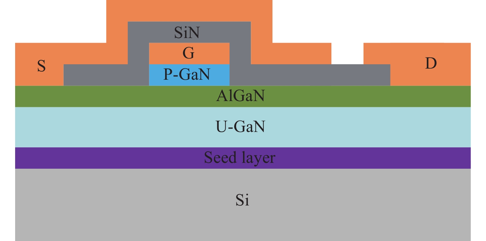
图 1 器件结构剖面图
Figure 1. Cross-section view of device structure
当前的GaN电子电力器件大多采用硅衬底,碳化硅衬底的器件电学性能更优,但其成本高,多用于射频器件的制造。衬底上的种子层有益于GaN材料的异质生长。U-GaN(Unintentional Doping GaN)层之上是与之形成二维电子气的AlGaN势垒层,P-GaN通过与势垒层形成耗尽区从而消除栅极下方沟道,达到关断的状态。栅金属之上是Si3N4钝化层,钝化层可以抑制势垒层表面态对沟道的影响,抑制电流崩塌效应[9]。源极场板(Source Field Plate)将栅极靠漏极一侧的电场向场板边沿推移,从而达到提高击穿电压的目的[10];漏极场板(Drain Field Plate)与源极场板的作用相似,但会增加miller电容[11],增大开关损耗。
-
晶体管开启过程中,栅极电流首先对栅源电容充电,当器件进入miller平台,栅源电压保持不变,栅极电流为栅漏电容充电,最终使得栅漏电压由负转正。当漏源电压降至最低,器件跳出miller平台。为方便栅极总电荷的仿真结果计算,将一定输入电压下的栅极总电荷分为3个部分:栅源电容上的正电荷、栅漏电容上的正电荷、栅漏电压由负转正过程中消耗的正电荷。
特殊的器件结构使GaN HEMT具有很小的栅极总电荷,为小尺寸GaN HEMT搭建输入级电路创造了条件。根据图1构建6.5 μm×1000 μm的原胞,对器件结构进行简单仿真。图2为输出特性曲线的仿真结果,栅极电压5 V时对应的最大电流密度为0.39 A/mm。以后续使用实际器件的脉冲峰值电流18 A为标准,取50个原胞并联,栅极电压上升至5 V时,对应320 pC的栅极总电荷。若信号源仅有20 mA的平均输出电流,利用Q=It粗略计算栅极电压上升至5 V所需的时间为16 ns,可以实现快速开关。实际的栅极总电荷还与器件的工艺、封装等有关,会高于仿真值。但仿真设置的电子迁移率较低,当前良好衬底的电子迁移率较高;且为保证较高的漏源击穿电压,设置的栅漏距离较大。因此,该尺寸的实际制造器件的过流能力可能比仿真结果强。仿真和粗略计算的结果表明,采用小尺寸GaN HEMT有望实现输入级的搭建。

图 2 输出特性曲线
Figure 2. Output characteristic curve
-
采用EPC (宜普电源转换公司)的两款GaN HEMT组成驱动电路,阈值电压皆为1.4 V。首先使用小尺寸的GaN HEMT搭建输入级,采用共漏极形式,如图3(a)所示。采用电容值与大尺寸GaN HEMT的输入电容相近的电容CL,与电阻RL并联作为共漏极输出负载,红色虚线框内为PCB上的电路。在实测系统中,信号源及电源与驱动电路之间的连接导线有较大寄生参数,根据其长度及PCB的布线估算电路中的寄生电感L1-3,Rin为信号源内阻,R1-3为寄生电阻,Rg为M1的栅极电阻,此外,还存在分布电容。
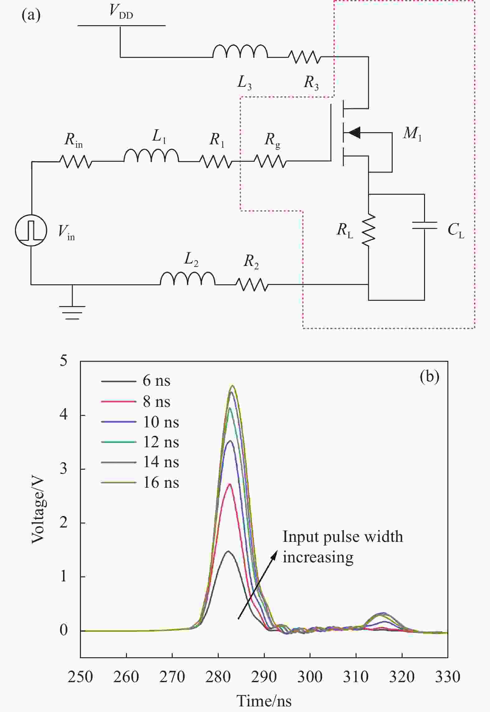
图 3 电路结构及仿真。 (a) 共漏极电路; (b) 源极电压仿真结果
Figure 3. Circuit structure and simulation. (a) Common drain circuit; (b) Source voltage simulation results
使用PSpice for TI对电路进行仿真,设置VDD为5 V,Vin频率为10 kHz、电平为5 V、上升沿下降沿为3 ns的脉冲信号,脉宽为6~16 ns,步长2 ns,M1源极电压仿真结果如图3(b)所示。源极电压波形形状基本不变,幅值由1.48 V增加至4.55 V,脉宽由5.9 ns增加至6.1 ns。若继续增加输入信号的脉宽,源极电压峰值不变,脉宽会略微展宽。仿真结果表明:该器件可以构建输入级电路,响应信号源输出,控制激光器放电回路的充放电。
-
使用美国宜普电源转换公司的两款GaN器件EPC2036与EPC2045,于PCB上搭建前文所述电路,加入激光器放电回路,驱动860 nm半导体激光器[6],如图4所示。选择的厂家仅生产大于10 mm×10 mm的PCB,电路实际有效尺寸为10 mm×6 mm。

图 4 板级驱动电路
Figure 4. Driver circuit on PCB
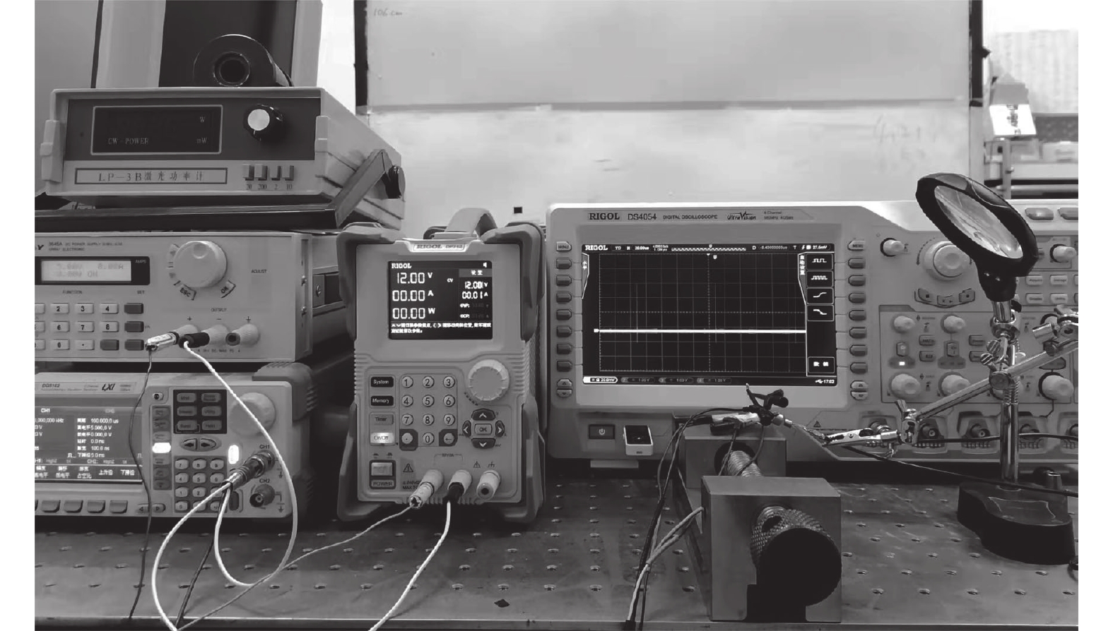
测试条件与仿真一致,但输入脉宽范围不同,为8~18 ns,由普源精电的信号发生器DG5102设置输出,激光器放电回路电压为12 V。测试系统如图5所示,采用连接示波器的光电探测器接收输出光信号,获得激光器输出光脉冲波形,如图6(a)~(f)所示,将波形导出为CSV格式文件,并使用绘图软件绘制,如图6(g)所示。通过观察示波器得到输出光脉冲脉宽,为4~8.8 ns。输入脉宽分别为16 ns和18 ns,对应的输出光脉冲曲线几乎重叠,因此,可以调整输出光脉冲的有效输入信号脉宽范围为8~16 ns。使用LP-3B激光功率计测量输出平均光功率,采用平均光功率与占空比相除的方式计算峰值功率,为3.7~8.3 W。

图 5 测试系统
Figure 5. Test system
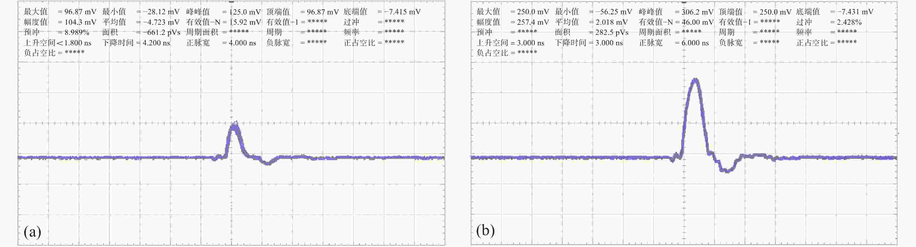
图 6 输出光波形。(a)~(f) 示波器显示波形;(g) 导出数据绘制波形
Figure 6. Output optical waveforms. (a)-(f) Waveforms displayed by an oscilloscope; (g) Waveforms drawn from the derived data
仿真结果与测试结果相近,输出信号形状近似不变、幅值变化,超出有效输入脉宽8~6 ns时增加输入脉宽,输出光脉冲的脉宽与幅值基本不变,超过一定值会出现多脉冲,文中仅使用第一个脉冲。放电回路的开关管存在开关时间,输出光脉冲相对于开关管栅极电压有一定的滞后,体现为输入信号脉宽可调范围的整体后移。测试结果中的输入级输出电压脉宽范围大于仿真结果中的范围,分别为5~7 ns、5.9~6.1 ns。原因可能是获取方式不同,前者是由示波器示数读出,而后者是由绘图软件得出。
M1使用的器件为100 V增强型GaN HEMT,其源漏击穿电压与源漏距离相关,而M1并不需要高的击穿电压。在电路的单片集成过程中,可以将M1的源漏距离缩小,不仅可以降低导通电阻,也可以减小并联的原胞个数,从而减小栅极总电荷,增加器件的响应速度。测试使用封装之后的激光器,回路中最大的寄生电感存在于激光器与电路的连接。若直接使用激光器管芯,可以降低寄生效应,增加输出光功率,笔者所在课题组已进行相关研究 [5,12]。
-
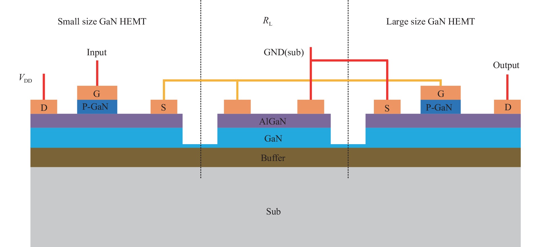
对于第2节提出的电路,其输出脉宽可调范围有限,需要新的电路结构,实现更大的输出脉宽可调范围。仍使用GaN HEMT搭建输入级,采用共源极结构。共源极结构将输入信号反相,需要添加一级再一次反相。从单片集成的角度考虑,P沟道GaN器件无疑是最好的选择,但P型GaN的空穴迁移率低,不利于制备P沟道功率器件。另一种办法是使用耗尽型和增强型的N沟道GaN器件构成反相器,但存在长时间导通的支路,受到散热与功耗的限制。最终选取Si PMOS与电阻构成中间级,如图7所示。最终的PCB尺寸为13 mm×11 mm。

图 7 输出光脉宽拓展电路
Figure 7. Circuit widening output light pulse width
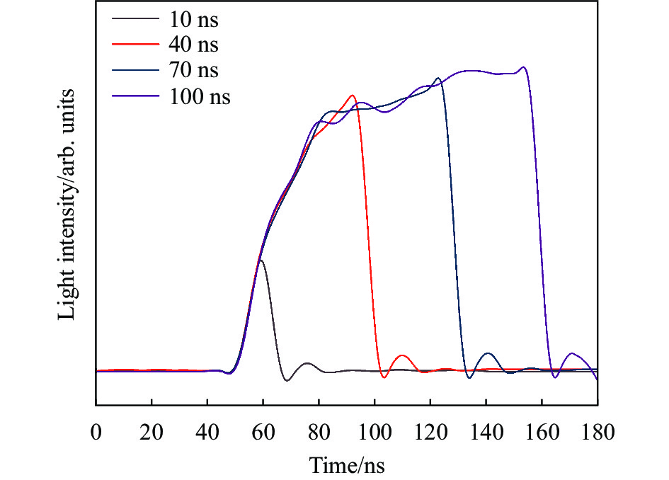
除输入信号脉宽外,其他测试条件与前文一致。输入脉宽为10~100 ns,步长为30 ns,将示波器测试结果导出并绘制波形,如图8所示。最窄输出光脉宽由示波器示数读出,为8.4 ns,此时输出光脉冲峰值功率为8.3 W,脉宽可调至100 ns以上。电源电压升至20 V,输入脉宽100 ns时,输出光峰值功率可达46.6 W。
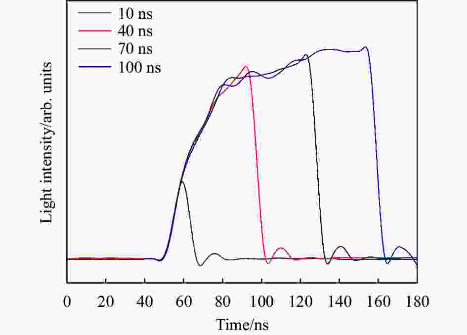
图 8 输出光波形
Figure 8. Output optical waveforms
测试结果表明,电路实现了更大的输出光脉宽可调范围。选取的M2响应速度较慢,在栅极电压较低时导通电阻较大,导致输出光脉冲上升沿的时间较长。可以选用响应速度更快、导通电阻更低的PMOS,使上升沿更加陡峭。
表1展示了文中提出电路与相关参考文献所提出电路的比较。脉冲宽度为输出光脉宽范围,峰值功率为输入脉宽100 ns时的输出光脉冲峰值功率,且参考文献[4]与[6]中激光器放电回路电压大于文中使用的20 V。测试采用GaN HEMT的尺寸分别为2.5 mm×1.5 mm、0.9 mm×0.9 mm,Si PMOS尺寸为2.8 mm×1.2 mm,若采用3.2节中的集成方法,集成的预期尺寸小于(2.5+0.9) mm×(1.5+0.9) mm。
表 1 对照表
Table 1. Comparison table
-
GaN器件的优点使得全GaN电路单片集成受到国内外广泛的研究。高校与企业陆续开发了基于不同增强型技术的集成工艺平台。其中,台积电提出了基于P-GaN增强型技术的100 V/650 V GaN-on-Si的工艺平台[13],可以集成电阻、二极管、低压逻辑晶体管、高压功率晶体管等元件。Chen等[14]提出了一款基于GaN工艺的电路,集成了驱动器及650 V增强型GaN HEMT。
第2节中提出的驱动电路,其所使用的电子元件除储能电容外,只有少数的晶体管和电阻,基于GaN工艺,容易实现单片集成,图9为其集成工艺结构示意图。

图 9 集成工艺结构示意图
Figure 9. Schematic diagram of integrated process structure
目前大多GaN外延片具有AlGaN势垒层,可以直接制备GaN HEMT,电阻与GaN HEMT制备工艺兼容,不需额外的工艺步骤。因此,整个驱动电路采用GaN HEMT的制备工艺即可完成单片集成。
第3.1节提出的电路比第2节提出的电路多出Si PMOS和电阻,采用Si PMOS工艺制备,电路中除电容外的其余元件采用GaN HEMT工艺制备,将两部分集成,即可完成电路的集成。集成方式采用3D堆叠式封装,将面积小的管芯倒扣在另一管芯上,笔者所在课题组已进行相关研究[6]。
-
针对半导体激光器驱动电路的可调窄脉宽、小型化的需求,基于GaN HEMT栅极总电荷小、导通电阻低等优点,提出激光器放电回路开关管采用GaN HEMT,并使用其构建输入级,完成栅极驱动器的功率放大功能。通过器件结构仿真与PCB电路测试,证实小尺寸GaN HEMT能够快速响应信号发生器输出的脉冲信号,并为后级开关管提供足够的栅极电流。该电路具有10 mm×6 mm的超小面积,可以驱动激光器输出脉宽为4~8.8 ns的光脉冲,实现了纳秒级窄脉宽。
为实现更大的输出光脉宽可调范围,提出另一款驱动电路,电路尺寸为13 mm×11 mm,实现了激光器驱动电路的小型化,打破了栅极驱动器控制激光器放电回路的模式。测试结果表明,该电路的输出光脉宽为大于8.4 ns可调,满足可调窄脉宽的需求。为实现进一步小型化,提出了电路的集成方法。提出的驱动电路结构简单、占用面积小、制作成本低,与提出的集成方法共同为小型的窄脉冲激光器驱动电路设计提供了新的方向。
Adjustable narrow pulse laser drive circuit using GaN HEMT
-
摘要: 为实现纳秒级的输出光脉宽,使用GaN HEMT作为激光器放电回路的开关管。由于GaN HMET的栅极总电荷小,提出使用小尺寸的GaN HEMT建立驱动电路的输入级,响应控制信号,控制放电回路开关管。搭建电路驱动860 nm激光器,并进行测试。放电回路电源电压为12 V,测试结果显示,最大输出光脉宽8.8 ns对应大于8 W的峰值功率,输出最小光脉宽为4 ns。为实现更大的脉宽可调范围,设计另一款电路并测试。该电路实现输出光脉宽大于8.4 ns可调,在电源电压20 V、输入信号脉宽100 ns的条件下,输出光峰值功率可达46 W。电路尺寸分别为10 mm×6 mm和13 mm×11 mm,为实现进一步小型化,对设计的电路提出了集成方法。提出的电路结构简单、容易实现集成且成本低,为窄脉冲激光器驱动电路的设计提供了新的思路。Abstract: GaN HEMT is used as the switch of the discharge circuit to achieve nanosecond pulse width. Due to the low total gate charge of GaN HMET, a GaN HEMT with small size is used to build the input stage of the driver circuit to respond to the control signal and control the discharge circuit switch. The circuit is built to drive the 860 nm laser and tested. The power supply voltage of the discharge circuit is 12 V, and the test results show that the maximum output pulse width of 8.8 ns corresponds to a peak power greater than 8 W, and the minimum output pulse width is 4 ns. Another circuit is designed and tested to achieve a larger pulse width adjustable range. The circuit realizes adjustable pulse width greater than 8.4 ns of output light. When the power supply voltage is 20 V and the pulse width of the input signal is 100 ns, the output optical peak power can reach 44 W. The area of the circuit is 10 mm×6 mm and 13 mm×11 mm. In order to realize further miniaturization of the drive circuit, a integration method is proposed for the two designed circuits. The proposed circuit is simple in structure, easy to realize integration and low in cost, which provides a new idea for the design of narrow pulse laser drive circuit.
-
Key words:
- semiconductor laser /
- driver circuit /
- GaN HEMT /
- narrow pulse /
- miniaturization
-
图 3 电路结构及仿真。 (a) 共漏极电路; (b) 源极电压仿真结果
Figure 3. Circuit structure and simulation. (a) Common drain circuit; (b) Source voltage simulation results
图 6 输出光波形。(a)~(f) 示波器显示波形;(g) 导出数据绘制波形
Figure 6. Output optical waveforms. (a)-(f) Waveforms displayed by an oscilloscope; (g) Waveforms drawn from the derived data
-
[1] Wei Y, Jiang S L, Sun G B, et al. Design of solid-state array laser radar receiving optical system [J]. Chinese Optics, 2020, 13(3): 517-526. (in Chinese) [2] Gao W K, Du X P, Wang Y, et al. Review of laser speckle target detection technology [J]. Chinese Optics, 2020, 13(6): 1182-1193. (in Chinese) doi: 10.37188/CO.2020-0049 [3] Wei C J, Yan R P, Li X D, et al. Research progress of sub-nanosecond lasers for 3D imaging lidar [J]. Optics and Precision Engineering, 2021, 29(6): 1270-1280. (in Chinese) doi: 10.37188/OPE.20212906.1270 [4] Ji Y F, Zhao B Q, Luo D X. Design of an ASIC for the driving and receiving part of dual-wavelength laser fuze [J]. Infrared and Laser Engineering, 2016, 45(7): 0705004. (in Chinese) doi: 10.3788/irla201645.0705004 [5] Han W, Zheng X, Zhao B Q. Design of miniaturized trans-mitting-receiving system for laser detection [J]. Infrared and Laser Engineering, 2017, 46(9): 0906008. (in Chinese) doi: 10.3788/IRLA201746.0906008 [6] Wang L J, Zhao B Q, Yang S X. Design of high current narrow pulse laser driving chip [J]. Infrared and Laser Engineering, 2021, 50(11): 20210034. (in Chinese) doi: 10.3788/IRLA20210034 [7] Khadar R A, Liu C, Soleimanzadeh R, et al. Fully vertical gan-on-si power MOSFETs [J]. IEEE Electron Device Letters, 2019, 40(3): 443-446. [8] Liero A, Klehr A, Hoffmann T, et al. GaN laser driver switching 30 a in the sub-nanosecond range[C]//European Microwave Conference. IEEE, 2016. [9] Zhong Y, Su S, Chen X, et al. Normally-off HEMTs with regrown p-gan gate and low-pressure chemical vapor deposition SiN [J]. IEEE Electron Device Letters, 2019, 40(9): 1495-1498. doi: 10.1109/LED.2019.2928027 [10] Godfrey D, Nirmal D, Arivazhagan L, et al. Investigation of AlGaN/GaN HEMT breakdown analysis with source field plate length for high power applications[C]//2020 5th International Conference on Devices, Circuits and Systems (ICDCS), 2020. [11] Soni A, Singh A, Shrivastava M. Novel drain-connected field plate GaN HEMT designs for improved VBD-Ron tradeoff and RF PA performance [J]. IEEE Transactions on Electron Devices, 2020, 67(4): 1718-1725. doi: 10.1109/TED.2020.2976636 [12] Chen Y C, Zhao B Q, Li W. High peak power semiconductor laser module for producing nanoseconds pulse [J]. Optics and Precision Engineering, 2009, 17(4): 695-700. (in Chinese) doi: 10.3321/j.issn:1004-924X.2009.04.001 [13] Lai J Y, Chen W J, Sun R Z, et al. Development of GaN monolithic power integrated circuits [J]. Electronics and Packaging, 2021, 21(2): 020103. (in Chinese) [14] Chen H Y, Kao Y Y, Zhang Z Q, et al. 33.1 A fully integrated GaN-on-Silicon Gate Driver and GaN Switch with temperature-compensated fast turn-on technique for improving relia-bility[C]//2021 IEEE International Solid- State Circuits Con-ference (ISSCC). IEEE, 2021. -

 点击查看大图

图(10) / 表(1)
计量
- 文章访问数: 305
- HTML全文浏览量: 131
- PDF下载量: 71
- 被引次数: 0