


-
红外探测技术作为一种可以快速获取图像并实时获取温度分布的非接触性探测技术,已经成为航空等领域中不可或缺的探测手段之一[1]。在诸多类型红外探测器中,测微辐射热计(Microbolometer)因具有工作范围宽,响应速率快、无需制冷,且器件结构简单、易于制备等优势被广泛关注。但器件灵敏度受限于热敏层材料的电阻温度系数(Temperature Coefficient of Resistance, TCR)。目前,国内外对于热敏电阻的热敏层材料研究和应用主要集中在氧化钒(Vanadium Oxide, VOx)和非晶硅(Amorphous Silicon, α-Si)材料[2],其电阻温度系数为−2.5%/K和−2%/K,限制了以此为热敏层的探测器灵敏度。
锰钴镍氧化物(MCNO)是一种具有AB2O4通式的立方尖晶石结构过渡金属氧化物,其中A为二价阳离子,占据四面体位置,B为变价阳离子,占据八面体位置。在材料制备过程中,Ni2+取代Mn2+进入八面体位置,处于八面体位置的Mn3+受到John-Teller畸变作用形成极化子,并且电子受到离子束缚作用成为小极化子,小极化子在声子的辅助作用下,在Mn3+和Mn4+离子间进行跃迁形成电荷传输[3],其TCR系数可达−4%/K[4]。Yokoyama等研究了不同化学计量比例的MCNO体块材料的电学特性,指出因制备方法差异可以导致MCNO材料中具有不同的晶体形态和占比,是影响电学性能的主要因素,占据八面体位置的Mn3+和Mn4+的比例直接影响MCNO材料的电导率[5]。与体块材料相比,MCNO薄膜与现有半导体工艺兼容性更好,制备性能优良的MCNO薄膜是开发高性能红外探测器的基础和关键。 MCNO薄膜制备方法通常有射频磁控溅射法 [6]、电子束蒸发法 [7]、化学溶液沉积法[8]等。黄志明课题组深入研究了化学溶液沉积法及射频磁控溅射法制备MCNO薄膜的工艺参数和薄膜光电性能,以及器件结构等[4,9−12],他们使用乙酸盐前驱体合成制备MCNO靶材,用于磁控溅射,制备了170 nm厚度(220)晶相为主的薄膜,光电性能表征显示该纳米薄膜为n-型半导体薄膜,TCR系数达到−3.50%/K,而电阻率较低(250 Ω·cm)[11]。F. Zhang等采用射频磁控溅射法分别比较了在400 ℃和600 ℃进行2 h退火对制备的MCNO薄膜光学性能的影响。通过比较发现,在400 ℃退火温度下制备的薄膜由于晶粒形态导致具有较低的电阻率和较宽的带隙[13]。W. Kong等采用射频磁控溅射法分别制备了不同厚度的薄膜,当MCNO薄膜厚度在265~887 nm时其择优取向为(400),TCR系数在−2.45%~ −3.10%/K之间;厚度在265~693 nm之间的薄膜负温度特性随厚度增加而增加,进一步增加厚度在693~887 nm之间时负温度特性则呈现出相反的现象,即随厚度减小而减小,当厚度为693 nm时负温度特性最佳,激活能最低;Mn阳离子分布的变化导致MCNO薄膜的电学性质发生变化[14]。R. Schmidt等比较了射频磁控溅射法、电子束蒸发法等制备出的NiMn2O4薄膜材料的微观结构形貌及光电学性质,射频磁控溅射法制备的薄膜可获得更强的结晶峰、更大的晶粒尺寸和更低的电阻率[15]。J. Wei等采用电子束蒸发法沉积Mn/Co/Mn/Ni/Mn多层膜,之后在空气氛围中进行退火,通过多层膜固态化合制备出(311)晶相择优取向的Mn1.56Co0.96Ni0.48O4薄膜材料[16]。该研究表明,随着退火温度的升高,薄膜结晶度得到提高,但对Mn3+和Mn4+的含量影响不大。由于使用电子束蒸发进行氧化物蒸镀时,到达衬底的组分比例可能会因为氧化物分解而改变,导致不能准确调控各元素比例,无法实现预期的化学计量比例和薄膜厚度,该方法可以避免氧化物分解带来的这些问题。
文中采用磁控溅射-电子束蒸发复合法制备MnO2-Co2O3/Ni/MnO2-Co2O3多层膜,并结合原位退火及后退火促进多层膜互扩散与固态化合,得到MCNO薄膜。方法意图在Mn、Co氧化物共溅射后,通过Ni扩散进入八面体位置调控薄膜的微观结构以及光电性能。详细研究了后退火对薄膜的光电性能影响,验证了该方法用于制备MCNO薄膜的可行性,讨论比较了方法的优势与不足,为进一步优化MCNO薄膜组份与掺杂配比以及结构-性能关系提供了新思路。
-
薄膜制备使用实验室自主研发的电子束-磁控溅射复合高真空镀膜设备,使用步进电机控制样品台180°翻转,实现在一个制备流程中进行磁控溅射共沉积和电子束蒸发交替镀膜,镀膜设备示意图如图1所示。首先采用脉冲直流电源(DC)和射频电源(RF)进行MnO2(DC靶,纯度99.9%)和Co2O3(RF靶,纯度99.9%)共溅射,然后使用电子束蒸发蒸镀Ni(纯度为99.99%,材料均来自中诺新材(北京)科技有限公司),MnO2-Co2O3共溅射层与Ni层交替重复制备多层膜(Sputter-Ebeam-Multilayer,以下简称“SEBM法”)。MnO2和Co2O3在指定功率下通过校准单位时间内薄膜的溅射厚度,得到溅射速率分别为0.23 Å/s (1 Å=10–10 m)和0.28 Å/s,使用膜厚晶振控制仪(INFICON SQC-310)进行电子束蒸镀速率(0.4 Å/s)和膜厚监控。

图 1 镀膜设备示意图
Figure 1. Schematic diagram of coating equipment
采用2 in(1 in=2.54 cm)面抛光蓝宝石衬底,在溅射前依次用丙酮(分析纯)、乙醇(分析纯)、超纯水(18.2 MΩ·cm)进行恒温50 ℃的超声清洗,之后用氮气吹干。溅射蒸镀MCNO薄膜工艺参数如表1所示。
表 1 溅射蒸镀MCNO薄膜工艺参数
Table 1. Process parameters of sputtering and evaporation of MCNO films
Deposition cycle Layer
sequenceDeposition layer material Deposition thickness/nm Deposition power/W Vacuum degree/Pa Deposition
temperature/℃Deposition atmosphere Cycle Ⅰ 1(Oxide co-deposition) MnO2(DC) 9.02 90 5×10⁻⁴ 450 Ar >99.9% Co2O3(RF) 11.47 100 2 (Metal) Ni 1.5 14.7 Cycle Ⅱ 3(Oxide co-deposition) MnO2(DC) 9.02 90 Co2O3(RF) 11.47 100 4 (Metal) Ni 1.5 14.7 ...... ...... ...... ...... ...... Termination layer 15(Oxide co-deposition) MnO2(DC) 9.02 90 Co2O3(RF) 11.47 100 完成MCNO薄膜沉积后,在450 ℃条件下原位退火1 h,之后对样片裂片,在管式炉空气氛围下,分别进行750、850、950 ℃后退火1 h,对应样品编号标记为无后退火(MCN0)、750 ℃后退火(MCN750)、850 ℃后退火(MCN850)和950 ℃后退火(MCN950)。
-
使用扫描电子显微镜(Scanning Electron Microscope/SEM, Hitachi S-4800,日本)进行MCNO薄膜材料的表面形貌表征。使用X射线衍射(X-ray Diffraction/ XRD, Bruker D8 Advance,德国)对不同编号的样品从5º~65º(2θ)进行扫描分析表征其晶相结构。薄膜材料的元素化合态结构表征(离子价态和阳离子分布情况)使用中国科学院苏州纳米技术与纳米仿生研究所纳米真空互联实验站(Nano-X)的X射线光电子能谱仪(X-ray Photoelectron Spectroscopy/XPS, Thermo Fisher ESCALAB Xi+,英国)对MCN0、MCN750、MCN850、MCN950进行Mn 2p、Co 2p、Ni 2p窄谱能级信号扫描,使用CasaXPS软件进行谱图分析,对C 1s峰(284.8 eV)进行能量校正。使用电子束蒸发蒸镀厚度为120 nm的金属电极,采用四探针法(Keithley 4200-SCS/F+SUSS PM8高精度探针台,美国)测量薄膜材料的常温电学性能,使用Nano-X的紫外-太赫兹全光谱光电测试探针台(E-probe, ModelCCR5-3T-(4TX-1MW40-6PORTS))进行220~300 K变温电阻测试。使用傅里叶变换红外光谱仪(FTIR, Nicolet 6700,美国)测量2.5~25 μm范围的薄膜透射率和吸光度。
-
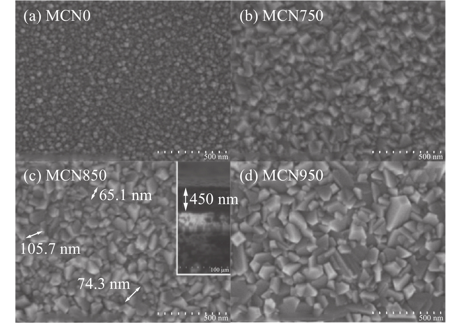
采用扫描电子显微镜观察了MCN0、MCN750、MCN850、MCN950的表面形貌,结果如图2所示,其中MCN850晶粒平均大小为81.7±24 nm,膜厚为450 nm。薄膜在不同退火温度条件下均呈现晶粒结构,MCNO的薄膜表面较为平整,但呈现晶粒尺寸最小,随着退火温度的增加,MCN750、MCN850、MCN950的表面晶粒尺寸逐渐增大,且分布均匀致密,结果表明,提高的沉积温度促进了晶粒的生长,薄膜结晶性更好。

图 2 MCNO薄膜样品的微观表面形貌
Figure 2. Microsurface morphology of MCNO thin film samples
图3给出了MCN0、MCN750、MCN850、MCN950薄膜的XRD表征曲线,薄膜呈现出多晶结构,MCNO的主要衍射峰分别为(111)、(220)、(311)、(222)、(400)、(511)[9],其中MCN0薄膜以(311)晶相为主。随着后退火温度升高,(111)、(222)晶相逐渐增强,并出现(511)晶相。MCNO薄膜在后退火前后表现出不同的择优取向性,由(311)向(111)晶面转变,其原因可能为薄膜材料在退火前后具有不同的最低表面能,而薄膜材料在具有最低表面能的晶面生长速率远远高于其他晶面[17]。因此,后退火工艺对文中采用的SEBM法制备的MCNO薄膜具有显著的结构调控作用。另一方面,在XRD谱图中仍然存在较强蓝宝石衬底的谱峰,说明薄膜的结晶度还未达到最佳,有待改进。

图 3 不同沉积温度的MCNO薄膜的XRD图谱
Figure 3. XRD patterns of MCNO films at different deposition temperatures
根据Scherrer公式:
$$ {D}_{G}=\frac{K\lambda }{\beta \mathit{\cos}\theta } $$ (1) 式中:K为Scherrer常数,当β为半高宽(Full Width at Half Maximum, FWHM)时K取0.89;λ为X射线CuKα波长(λ=0.15 nm)。需要说明的是,由于Scherrer公式计算所得为单晶粒尺寸,而SEM中表征的可能为团簇的晶粒尺寸,因此两者呈现的尺寸出现不一致。MCN750、MCN850、MCN950在(111)晶相的半高宽(FWHM)分别为0.77、0.48、0.36,计算得到相应的平均晶粒尺寸分别为11.16、17.1、23.87 nm,晶粒尺寸随着退火温度升高而增大,该趋势与SEM结果一致。根据布拉格公式:
$$ {D}_{L}=\frac{n\lambda }{2\mathrm{sin}\theta }=\frac{\mathrm{\lambda }\sqrt{\left({l}^{2}+{k}^{2}{+h}^{2}\right)}}{2\mathrm{sin}\theta } $$ (2) 计算可得晶格常数分别为8.71 Å、8.70 Å和8.69 Å,与相关报道一致。当退火温度从750 ℃上升到950 ℃,(111)衍射峰向高角度迁移,晶格尺寸降低。表2总结了MCN750、MCN850、MCN950在(111)衍射峰位的半峰宽、晶粒尺寸和晶格常数。
表 2 MCN750、MCN850、MCN950在(111)衍射峰位的半峰宽、晶粒尺寸和晶格常数
Table 2. Half-peak width, grain size and lattice constant of MCN750, MCN850 and MCN950 at (111) diffraction peak position
Sample FWHM
(111)Peak position
(2θ)/(°)Grain size/
nmLattice constant/
ÅMCN750 0.77 18.93 11.16 8.71 MCN850 0.48 18.93 17.91 8.70 MCN950 0.36 18.97 23.87 8.69 -
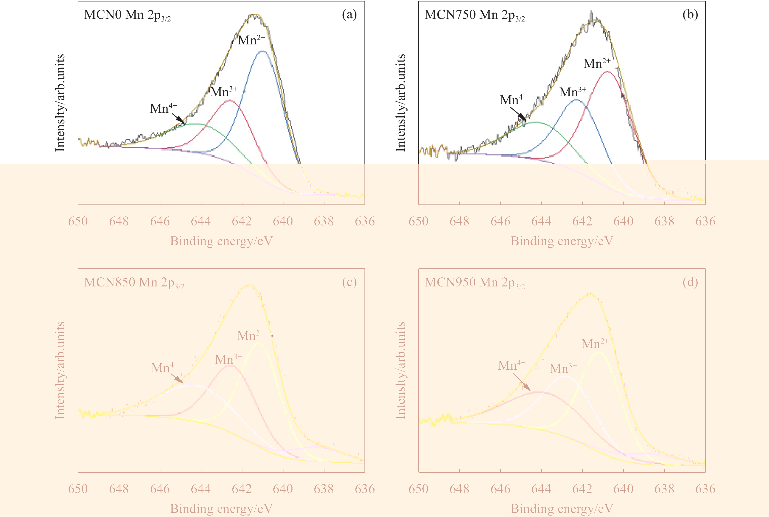
MCNO中的Mn3+和Mn4+的之间的电荷传输对温度具有很大的依赖性,使得薄膜具有热敏性质。对Mn 2p、Co 2p、Ni 2p的XPS谱峰进行了定量拟合分析。使用Casa XPS软件对MCN0、MCN750、MCN850、MCN950的Mn 2p3/2谱图进行拟合分析,图4(a)~(d)呈现的Mn2+(641.1 eV)、Mn3+(642.6 eV)和Mn4+(644.1 eV)的半峰宽(FWHM)别为3.39、3.43、3.76、3.78,大于MnO(3.2 eV)、Mn2O3(3.0 eV)和MnO2(2.5 eV)等单氧化态的Mn阳离子半峰宽[18],结果表明所制备的MCN薄膜含有多价Mn阳离子。计算Mn2+、Mn3+和Mn4+离子峰面积得到各离子的含量比,具体数值见表3。从数据中可以看出,Mn4+/Mn3+的比值随着退火温度的升高而增大,与相关文献报道趋势一致[19]。

图 4 Mn 2p3/2的XPS谱拟合
Figure 4. XPS spectrum fitting of Mn 2p3/2
表 3 MCN0、MCN750、MCN850、MCN950的Mn离子价态分布及相对比例
Table 3. Valence state distribution and relative proportion of MCN0, MCN750, MCN850, and MCN950
Sample Mn2+∶Mn3+∶Mn4+ Mn4+/Mn3+ MCN0 0.53∶0.27∶0.20 0.74 MCN750 0.49∶0.29∶0.21 0.75 MCN850 0.41∶0.26∶0.25 0.96 MCN950 0.38∶0.27∶0.30 1.11 图5(a)为Ni 2p的XPS谱图,图中MCN0没有明显的Ni峰,MCN750、MCN850和MCN950中Ni 2p3/2的谱峰位置显示在~854.5 eV,存在形式为Ni2+,且其强度随着退火温度的增加而增强;计算比较MCN750、MCN850和MCN950的谱峰积分面积(868~851 eV),得到MCN850和MCN950的谱峰面积较MCN750约增加1.5倍。由于X射线光电子能谱仪对样品表面的探测深度约为10 nm,Ni强度的增加说明在Mn、Co氧化层下的Ni向Mn、Co氧化层中扩散,且扩散随着退火温度的升高而增多,从Ni 2p的谱峰位置及强度变化趋势可以说明Ni扩散明显地进入Mn、Co氧化物层,并形成化合态。图5(b)为Co 2p的XPS谱图,Co 2p3/2的谱峰位置在~780.0 eV,显示主要存在形式为Co2+,与溅射靶材化合态(Co2O3)相比,Co离子的主要存在形式由III价转化为II价,进一步说明退火促进了多层膜的固态化合,形成 MCNO化合物,与XRD结果相符。

图 5 MCN0、MCN750、MCN850、MCN950的Ni 2p (a)和Co 2p (b)的XPS谱
Figure 5. XPS spectra of MCN0, MCN750, MCN850, MCN950 of Ni 2p (a) and Co 2p (b)
-
采用四探针法测试得到常温下MCN0、MCN750、 MCN850和MCN950的线性伏安特性曲线,得到薄膜的电阻分别为1.17×10¹⁰ Ω、1.50×10⁷ Ω、1.43×10⁷ Ω和2.4×10⁷ Ω,对应电阻率分别为5.27×10⁵ Ω·cm、647.86 Ω·cm、642.19 Ω·cm和1100.30Ω·cm。
因MCN0薄膜样品在温度较低时不具有线性伏安特性曲线,仅对MCN750、MCN850和MCN950样品在220~300 K温度区间内采用二探针法进行变温电阻测试。电阻值Ω与测试温度T之间的关系及曲线拟合如图6(a)所示。从图中可以看出,MCN750、MCN850、MCN950的薄膜的电阻随着温度升高呈指数下降,具有典型的负温度系数(Negative Temperature Coefficient, NTC)特性。
薄膜电阻率和温度之间的关系可以表示为:

图 6 (a) MCN750、MCN850和MCN950薄膜样品电阻与温度之间的关系;(b) MCN750、MCN850和MCN950薄膜样品ln(ρ/T)与(1/T0.5)(空心线)和 ln(ρ/T)与(1000/T)(实心线)的关系图
Figure 6. (a) Relationship between resistance and temperature of MCN750, MCN850 and MCN950 film samples; (b) Relationship between ln (ρ/T) and (1/T0.5) (open line) and ln (ρ/T) and (1000/T) (solid line) for MCN750, MCN850 and MCN950 film samples
$$ \rho \left(T\right)={CT}^{\alpha }\exp{\left(\frac{{T}_{0}}{T})\right)}^{p} $$ (3) 式中:C为常数;T为绝对温度;T0为特征温度。MCNO薄膜材料的导电机制主要以Mn3+和Mn4+之间小极化子的传导跃迁为主。小极化子的跃迁传导机制可以分为近邻跃迁模型(Nearest Neighbor Transition Model,NNH)和为变程跃迁模型(Variable Range Transition Model,VRH)[3]。当α=p=1时,为近邻跃迁模型;当α=2p时,为变程跃迁模型。Mn3+和Mn4+之间小极化子跃迁所需的能量被称为激活能(Activation Energy, Ea),计算公式如下:
$$ {{{E}}_a} = {K_B}{T_0} $$ (4) 式中:T0为特征温度,是反应材料电阻对温度灵敏性的一个参数;KB为玻尔兹曼常数。对公式(3)取对数得到ln($ \rho $ /T)与(1/T0.5)的关系曲线(图6(b)中a线)。从图中可以看出,在三种退火条件下,ln($ \rho $ /T)与(1/T0.5)均呈现线性关系,符合α=2p时小极化子跃迁传导VRH模型[20]。做ln($ \rho $/T)与(1000/T)的关系图(图6(b)中b线),在220~300 K温度区间进行线性拟合得到曲线斜率,代入公式(3)得到MCN750、MCN850和MCN950的特征温度均为3361 K,代入公式(4)得到MCN750、MCN850和MCN950激活能为0.29 eV。
薄膜的电阻温度系数TCR可以表示为:
$$ TCR=\frac{{R}_{T}-{R}_{T0}}{{R}_{T0}({T}-{T}_{0})}=\frac{{\mathrm{d}}R}{R\times {\mathrm{d}}T} $$ (5) 根据公式(5)计算得到在室温(295 K)下MCN750、MCN850和MCN950的TCR系数分别为−1.95%/K、−4.20%/K和−4.14%/K,其中MCN850的TCR系数绝对值最高。该结果与表3中的Mn4+/Mn3+比值对照,MCN750、MCN850和MCN950的Mn4+/Mn3+比值分别为0.75,0.96和1.11,MCN850的Mn4+/Mn3+最接近1,符合Mn4+和Mn3+含量比值趋近1时电阻率最低、电学性能最佳的预期[21]。
-
采用傅里叶变换红外光谱仪分别测试MCN0、MCN750、MCN850、MCN950薄膜在2.5~25 μm波长范围内透射率。如图7(a)所示,薄膜在6~14 μm光谱范围内透射率随着波长的增长逐渐减小,在波段6~8.5 μm光谱范围内分别在7.0 μm、7.6 μm和8.2 μm存在吸收峰。透射率和吸光度(Absorbance)之间的关系可以表示为$ A = - \lg T $。计算得到该波段内的吸光度谱图如图7(b)所示。在波段7.5~8.2 μm范围内,MCN0、MCN750、MCN850、MCN950的最大吸光度分别为1.45、1.47、1.50、1.51。

图 7 MCN0、MCN750、MCN850、MCN950薄膜的透射光谱(a)和吸光度光谱(b)
Figure 7. Transmission spectrum (a) and absorbance spectrum (b) of MCN0, MCN750, MCN850, MCN950 films
虽然各样品的透射/吸收性能相近,但增加后退火工艺后,薄膜对光的吸收能力有所增强。其原因可能是后退火过程中,高温促进薄膜内部晶粒的合并与尺寸增大,减少了晶界数量和内部缺陷,晶体质量的提高可以降低对光的散射,提高薄膜对光的吸收能力。MCN950的吸光度值最高,与其在SEM及XRD表征结果中具有晶粒尺寸最大、(111)半峰宽最小、结晶性最好的结果一致。
采用常规磁控溅射方法制备MCNO薄膜,均相反应方法制备靶材,通过磁控溅射在衬底上形成具有靶材化学计量比例的MCNO薄膜,具有良好的均匀性和结晶度,得到TCR系数最大为−4.09%/K,电阻率为648~890 Ω·cm,激活能为0.29~0.31 eV[22]。与之相比,文中采用SEBM法,即MnO2和Co2O3共溅射,然后使用电子束蒸发蒸镀Ni,MnO2-Co2O3共溅射层与Ni层交替重复、逐层镀膜,再通过原位退火及后退火促进多层膜互扩散和固态化合。在850 ℃后,退火得到的薄膜TCR系数高达−4.20%/K,电阻率为642.19 Ω·cm,激活能为0.29 eV,并且在7.5~8.2 μm中红外波段具有较高吸光度。值得注意的是,现有文献中MCNO薄膜以(400)或(200)晶面的择优取向为主,而SEBM法制备的薄膜以(111)晶面为主。究其原因,制备方法差异可能是导致SEBM法的薄膜结构-性能不同于现有文献报道的主要因素。此外,MnO2-Co2O3/Ni/MnO2-Co2O3多层膜在退火过程中互扩散及固态化合亦可能生成亚稳态,产生区别于热力学稳定体系的材料体系和优良性能[22]。另一方面,文中使用拉曼对样品Mn-O峰(100~1000 cm−1)进行多点测量(数据未显示),得到的谱峰强度存在较大差异,据此判断SEBM法制备的MCNO薄膜均匀性与采用化学溶液法和固定成分靶材的射频磁控溅射法相比可能较差。同时,XRD谱图中呈现出较强的衬底峰,说明结晶度未达到最佳,有待进一步优化。
-
文中采用SEBM法结合退火工艺制备亚微米 厚度的MCNO薄膜,研究了后退火工艺对薄膜性能的影响。结果显示,该薄膜具有MCNO薄膜的结构和负温度系数特性,化合态分析与电学特征相符,验证了方法用于沉积MCNO薄膜具有较高的可行性,为优化和研发不同组分和掺杂配比的薄膜及其结构-性能关系提供了新思路。与现有文献相比,其负温度系数和吸光度较高,电阻率适中,为制备高灵敏度的红外探测器件提供了基础。另一方面,薄膜结晶度和均匀性相对较差,后续可以进一步通过优化原位沉积温度、沉积氛围以及退火工艺进行改善。对该方法体系的热力学行为特征和电学输运特性有待进一步深入研究,将有助于研发性能更优的MCNO薄膜材料体系。
致 谢 :感谢中国科学院苏州纳米技术与纳米仿生研究所纳米真空互联实验站和创新实验室提供测试技术支持。
Preparation of MCNO thin films by solid-state reaction of oxide-metal multilayers
-
摘要: 红外热成像技术具有高度实用性、灵敏性和可靠性等优点,在航空、医疗等多个领域发挥着重要作用。相较于其他类型的非制冷红外探测器,测微辐射热计(Microbolometer)具有工作范围宽、响应速率快且器件结构简单等优点。相较于非晶硅和氧化钒等常见热敏层材料,立方尖晶石结构的过渡金属氧化物锰钴镍氧化物(Mn-Co-Ni-O,MCNO)具有更高的TCR系数。使用磁控溅射法-电子束蒸发复合法在蓝宝石(Al2O3)衬底上制备MCNO薄膜,结合XRD、SEM和电学性能测试,分析和探讨了工艺条件对其性能的影响。研究结果表明,在450 ℃沉积 5 h得到厚度为450 nm的MCNO薄膜样品,随后在真空腔内原位退火1 h,再使用管式退火炉在空气氛围中进行60 min 850 ℃后退火,MCNO薄膜呈现出良好性能,(111)晶相的XRD半峰宽为0.48,晶格常数为8.71 Å(1 Å=10–10 m),晶粒平均大小为81.7±24 nm。使用四探针法测试MCNO薄膜室温下电阻率为642.19 Ω·cm,室温下(295 K)电阻温度系数(Temperature Coefficient of Resistance, TCR)系数为−4.20%/K。在6~8.5 μm波长范围内,最高吸光度为1.50。研究结果验证了所提出的多层复合方法用于制备MCNO薄膜的可行性,为进一步优化MCNO薄膜组份与掺杂配比以及结构-性能关系提供了新思路。Abstract:
Objective Microbolometers offer advantages such as wide working range, fast response time, and simple device structure. The working principle is that infrared radiation incidents on the absorption layer, generating thermal energy which is then transferred to the thermosensitive material. The thermosensitive material changes its electrical resistance upon absorbing the heat and thus produces a change in output signal detected by the readout circuit. The thermosensitive layer has a significant impact on the performance of microbolometer. Currently, the main industrial materials for the thermosensitive layer are vanadium oxide and amorphous silicon, with a general temperature coefficient of resistance (TCR) of −2%/K. Compared to vanadium oxide and amorphous silicon, manganese cobalt nickel oxide (MCNO) with high TCR coefficients has great potential in uncooled infrared detector applications. Unlike most MCNO thin films prepared by magnetron sputtering of a stoichiometric compound, this paper reports the synthesis of MCNO by combining magnetron sputtering and electron beam evaporation. MnO2 and Co2O3 were co-sputtered initially, followed by e-beam evaporation of Ni. Multilayers of MnO2-Co2O3 oxides and Ni were thus deposited alternatively and subjected to in-situ and/or post-annealing to promote interdiffusion and the formation of MCNO compound. The objective was to investigate the feasibility of the new fabrication method based on solid state synthesis. The prepared thin films showed good crystallinity and negative temperature coefficient of resistance, indicating that the proposed method could be applied to further fine-tuning the compositions of MCNO thin films in the future. Methods Thin films were prepared using a magnetron sputtering-electron beam evaporation hybrid method using a laboratory-developed high vacuum coating unit, where an e-gun and two magnetron sputtering targets coexisted in the same chamber. The sample stage was controlled by a stepper motor for 180-degree rotation, thus enabling alternative up-facing magnetron co-sputtering and down-facing electron beam evaporation in a single fabrication process. Sapphire substrate was cleaned with acetone, ethanol, and deionized water sequentially, dried up with blowing N2 gas, and pre-heated in the vacuum chamber at 450 ℃ for one hour prior to the deposition. To study the effect of post-annealing on the performances of MCNO thin films, the as-deposited thin film samples were first annealed in-situ in the vacuum chamber for an hour, then annealed in a tube furnace in the air at 750 ℃, 850 ℃, and 950 ℃ respectively. The surface morphology of the resultant MCNO thin films were characterized using scanning electron microscopy (SEM). The crystal phase structure was characterized using X-ray diffraction analysis. The resistance at variable temperature from 220 K to 300 K was measured using a two-probe setup on a UV-THz full-spectrum photoelectric test probe stage. The transmittance and absorbance of the thin films were examined using Fourier-transform infrared spectroscopy (FTIR) in the 2.5-25 μm range. Results and Discussions XRD characterization showed that the thin films exhibited polycrystalline structures with different preferential orientations as the annealing temperature increased. The primary crystal orientation obtained was (111), and the peak intensity increased with increasing annealing temperature. SEM characterization showed that the grain size of the thin film increased with increasing annealing temperature, consistent with the XRD results. FTIR characterization showed that the absorbance of the thin films increased toward the long wavelength in the 6-8.5 μm range and reached 1.50 for the sample annealed at 850 ℃. XPS quantification showed that the ratio of Mn4+/Mn3+ in the film increased with increasing annealing temperature. All thin films exhibited ohmic characteristic curves measured with four-point probe method at room temperature. It was shown that the samples annealed at 750, 850, and 950 ℃ respectively exhibited characteristic negative temperature coefficients, with calculated TCR of −1.95%/K, −4.20%/K, and −4.14%/K accordingly. The high TCR could be attributed mainly to the fabrication method, as solid phase synthesis of MCNO thin films via layer-by-layer deposition could result in metastable states in the thin films, thereby achieving better TCR and absorbance unobtainable in systems of thermal equilibrium. Conclusions This paper explored a magnetron sputtering-electron beam evaporation hybrid method based on solid phase synthesis to fabricate MCNO thin films. The impact of post-annealing on the properties of the thin films was investigated. Thin films prepared with optimized processing parameters showed high absorbance and excellent negative temperature coefficient of resistance. This study demonstrated the feasibility of fabricating MCNO films using the proposed method, offering a new approach for further development of MCNO thin films with optimal composition-property relationship. -
图 3 不同沉积温度的MCNO薄膜的XRD图谱
Figure 3. XRD patterns of MCNO films at different deposition temperatures
图 5 MCN0、MCN750、MCN850、MCN950的Ni 2p (a)和Co 2p (b)的XPS谱
Figure 5. XPS spectra of MCN0, MCN750, MCN850, MCN950 of Ni 2p (a) and Co 2p (b)
图 6 (a) MCN750、MCN850和MCN950薄膜样品电阻与温度之间的关系;(b) MCN750、MCN850和MCN950薄膜样品ln(ρ/T)与(1/T0.5)(空心线)和 ln(ρ/T)与(1000/T)(实心线)的关系图
Figure 6. (a) Relationship between resistance and temperature of MCN750, MCN850 and MCN950 film samples; (b) Relationship between ln (ρ/T) and (1/T0.5) (open line) and ln (ρ/T) and (1000/T) (solid line) for MCN750, MCN850 and MCN950 film samples
图 7 MCN0、MCN750、MCN850、MCN950薄膜的透射光谱(a)和吸光度光谱(b)
Figure 7. Transmission spectrum (a) and absorbance spectrum (b) of MCN0, MCN750, MCN850, MCN950 films
表 1 溅射蒸镀MCNO薄膜工艺参数
Table 1. Process parameters of sputtering and evaporation of MCNO films
Deposition cycle Layer
sequenceDeposition layer material Deposition thickness/nm Deposition power/W Vacuum degree/Pa Deposition
temperature/℃Deposition atmosphere Cycle Ⅰ 1(Oxide co-deposition) MnO2(DC) 9.02 90 5×10⁻⁴ 450 Ar >99.9% Co2O3(RF) 11.47 100 2 (Metal) Ni 1.5 14.7 Cycle Ⅱ 3(Oxide co-deposition) MnO2(DC) 9.02 90 Co2O3(RF) 11.47 100 4 (Metal) Ni 1.5 14.7 ...... ...... ...... ...... ...... Termination layer 15(Oxide co-deposition) MnO2(DC) 9.02 90 Co2O3(RF) 11.47 100  下载: 导出CSV
表 2 MCN750、MCN850、MCN950在(111)衍射峰位的半峰宽、晶粒尺寸和晶格常数
Table 2. Half-peak width, grain size and lattice constant of MCN750, MCN850 and MCN950 at (111) diffraction peak position
Sample FWHM
(111)Peak position
(2θ)/(°)Grain size/
nmLattice constant/
ÅMCN750 0.77 18.93 11.16 8.71 MCN850 0.48 18.93 17.91 8.70 MCN950 0.36 18.97 23.87 8.69
下载: 导出CSV
表 3 MCN0、MCN750、MCN850、MCN950的Mn离子价态分布及相对比例
Table 3. Valence state distribution and relative proportion of MCN0, MCN750, MCN850, and MCN950
Sample Mn2+∶Mn3+∶Mn4+ Mn4+/Mn3+ MCN0 0.53∶0.27∶0.20 0.74 MCN750 0.49∶0.29∶0.21 0.75 MCN850 0.41∶0.26∶0.25 0.96 MCN950 0.38∶0.27∶0.30 1.11
下载: 导出CSV
-
[1] Rogalski A. Recent progress in infrared detector technologies [J]. Infrared Physics & Technology, 2011, 54(3): 136-154. doi: 10.1016/j.infrared.2010.12.003 [2] Lee J, Rodriguez C, Blackwell R. BAE Systems' 17 mm LWIR camera core for civil, commercial, and military applications [C]//SPIE, 2013, 8704: 459-464. [3] Schmidt R, Basu A, Brinkman A W, et al. Electron-hopping modes in NiMn2O4+ δ materials [J]. Applied Physics Letters, 2005, 86(7): 73501-73501. doi: 10.1063/1.1866643 [4] Zheng G, Jiang L, Zhou W, et al. Mechanism of high qualified Mn-Co-Ni-O thin films grown at low temperature [J]. Applied Surface Science, 2024, 644: 158672. doi: 10.1016/j.apsusc.2023.158672 [5] Yokoyama T, Abe Y, Meguro T, et al. Preparation and electrical properties of sintered bodies composed of monophase spinel Mn_<(2–X)>Co_<2X>Ni_<(1–X)>O_4 (0 ≦ X≦ 1) derived from rock-salt-type oxides[J]. Japanese Journal of Applied Physics , 1996, 35(11): 5775-5780. [6] Li R, Fu Q, Zou X, et al. Mn-Co-Ni-O thin films prepared by sputtering with alloy target [J]. Journal of Advanced Ceramics, 2020, 9(1): 64-71. doi: 10.1007/s40145-019-0348-y [7] Schmidt R, Brinkman A W. Preparation and characterisation of NiMn2O4 films [J]. International Journal of Inorganic Materials, 2001, 3(8): 1215-1217. doi: 10.1016/s1466-6049(01)00131-3 [8] Gao Y Q, Zhang Z B, Zhou W, et al. Mechanism of Cu dopant in transition metal oxide Mn1.56Co(0.96- x)Ni0.48CuxO4+ δ (0≤x≤0.2) thin films [J]. Thin Solid Films, 2020, 701: 137935. doi: 10.1016/j.tsf.2020.137935 [9] Wu J, Huang Z, Hou Y, et al. Structural, electrical, and magnetic properties of Mn2.52- xCoxNi0.48O4 films [J]. Journal of Applied Physics, 2010, 107(5): 053716. doi: 10.1063/1.3309780 [10] Zhou W, Yin Y, Wu J, et al. Improvements in electrical properties, low frequency noise and detection performance of a Mn-based bilayer thin film infrared detector [J]. Sensors and Actuators A: Physical, 2018, 283: 196-203. doi: 10.1016/j.sna.2018.10.002 [11] Huang Z, Zhou W, Ouyang C, et al. High performance of Mn-Co-Ni-O spinel nanofilms sputtered from acetate precursors [J]. Scientific Reports, 2015, 5(1): 10899. doi: 10.1038/srep10899 [12] 张飞, 欧阳程, 周炜, 等. 退火对 Mn-Co-Ni-O 薄膜器件性能的影响 [J]. 红外与毫米波学报, 2016, 35(1): 287-293. doi: 10.11972/j.issn.1001-9014.2016.03.007 Zang Fei, Ou Yangcheng, Zhou Wei, et al. Annealing effect on the properties of Mn-Co-Ni-O film detector [J]. Journal of Infrared and Millimeter Waves, 2016, 35(1): 287-293. (in Chinese) doi: 10.11972/j.issn.1001-9014.2016.03.007 [13] Zhang F, Ju J, Huo D, et al. Photoelectric and photocatalytic properties of long-time annealing Mn–Co–Ni–O thin film [J]. Journal of Materials Science:Materials in Electronics, 2023, 34(6): 523. doi: 10.1007/s10854-023-09934-2 [14] Kong W, Wei W, Gao B, et al. A study on the electrical properties of Mn-Co-Ni-O thin films grown by radio frequency magnetron sputtering with different thicknesses [J]. Applied Surface Science, 2017, 423: 1012-1018. doi: 10.1016/j.apsusc.2017.06.290 [15] Schmidt R, Basu A, Brinkman A W. Production of NTCR thermistor devices based on NiMn2O4+ δ [J]. Journal of the European Ceramic Society, 2004, 24(6): 1233-1236. doi: 10.1016/s0955-2219(03)00415-1 [16] Wei J H, Ren W, Lu H, et al. Synthesis of medium entropy Mn1.56Co0.96Ni0.48O4 films by solid-state reaction [J]. Journal of Solid State Chemistry, 2022, 306: 122742. [17] Ji G, Chang A, Xu J, et al. Low-temperature (<300 ℃) growth and characterization of single-[100]-oriented Mn-Co-Ni-O thin films [J]. Materials Letters, 2013, 107: 103-106. doi: 10.1016/j.matlet.2013.05.079 [18] Zhou W, Wu J, Ouyang C, et al. Optical properties of Mn-Co-Ni-O thin films prepared by radio frequency sputtering deposition [J]. Journal of Applied Physics, 2014, 115(9): 093512. doi: 10.1063/1.4867439 [19] Wu J, Huang Z, Zhou W, et al. Investigation of cation distribution, electrical, magnetic properties and their correlation in Mn2– xCo2 xNi1– xO4 films [J]. Journal of Applied Physics, 2014, 115(11): 113703. doi: 10.1063/1.4868683 [20] Zhou W, Zhang L, Ouyang C, et al. Micro structural, electrical and optical properties of highly (220) oriented spinel Mn-Co-Ni-O film grown by radio frequency magnetron sputtering [J]. Applied Surface Science, 2014, 311: 443-447. doi: 10.1016/j.apsusc.2014.05.088 [21] Yin Y, Wu J, Zhou W, et al. Effects of deposition temperature on microstructure, cation distribution and electrical properties of Mn1.56Co0.96Ni0.48O4 thin films grown by RF magnetron sputtering [J]. Journal of Alloys and Compounds, 2020, 822: 153705. [22] Stein A, Keller S W, Mallouk T E. Turning down the heat: Design and mechanism in solid-state synthesis [J]. Science, 1993, 259(5101): 1558-1564. doi: 10.1126/science.259.5101.1558 -

 点击查看大图

计量
- 文章访问数: 14
- HTML全文浏览量: 2
- PDF下载量: 4
- 被引次数: 0

