


-
随着5G时代的到来,移动互联网、大数据、云计算等技术飞速发展,数据使用量迅速暴涨,进一步提高信息传输速率和容量是目前最为迫切的需求。而目前对单元器件的研究已趋近成熟,利用硅基光电子集成技术将多种功能器件,例如光调制器[1]、光探测器[2-3]以及光传感器[4]等集成在同一个芯片上[5],实现光电子器件小型化和多功能化,对未来高速大容量光通信领域以及光电集成领域具有重要意义。
为了提高通信速率和传输容量,可以采用模分复用光通信系统,而光调制器与模分复用器是模分光通信系统的关键器件[6]。近年来,由于硅基电光调制器尺寸小,便于集成,成为了研究热点。常见的硅基电光调制器有脊型波导调制器[7]、马赫-曾德尔型调制器(MZM)[8-9]、光子晶体谐振腔型调制器(PCR)[10-11]等。脊型波导调制器和马赫曾德尔型调制器驱动电压较高、尺寸较大,不利于集成;PCR型调制器驱动电压较低、尺寸小,适合多功能器件的集成。2019年,周昊天等人[11]提出了一种基于AAH谐振腔的紧凑型电光调制器,该电光调制器尺寸仅为9.03 μm,易于集成,且消光比高达29.13 dB。因此,采用PCR型调制器更适合集成。同时,近年来片上波导型模分复用器也得到了广泛的研究。模分解复用器件主要分为绝热耦合(AC)[12]型、多模干涉(MMI)[13]型、非对称Y 结(Y-Junctions)型[14]、光栅辅助反向耦合(GACC)[15]型、非对称定向耦合(ADC)[16]型等。AC型和MMI型器件虽然耦合长度短,尺寸小,但只支持两个模式的传输,不具有扩展性;非对称Y结型虽易于级联,但其结构设计较为复杂;GACC型器件虽解决了上述问题,但其工作带宽太窄;而ADC型器件不仅结构简单、器件尺寸较短,还易于级联扩展。2020年,伊朗西拉大学的Kolsoom Mehrabi等人[16]提出了一种基于非对称弯曲定向耦合结构的两模式模分复用器,该器件耦合长度短,在1550 nm的通信波长下损耗为0.87 dB,串扰为−21.8 dB,模式转换效率达98.3%。综合考虑,非对称定向耦合型模分复用器件因其结构简单、器件尺寸短,还易于级联扩展,更适合于器件集成 。
近年来,将光通信系统中的电光调制器模块与模分复用器模块进行光电集成的研究也不断涌现。2018年,Jiangbing Du[17]等人制作了4通道硅微环调制器组装芯片,用于空分复用光互连,该器件消光比为13~16 dB,总插损高达22 dB,有待进一步降低。2020年,项彤等人[18]设计了一种硅基电光调制与模分复用集成器件,该器件插损为0.46 dB,但串扰较大,且仅能调制一个波长。为了进一步提高通信容量和集成器件性能,文中提出一种基于光子晶体的双波长电光调制和模分复用集成器件,该器件的工作波长为1552.1 nm和1556.1 nm,可以完成两个波长的TE0模通断调制及TE0模和TE1模的两模式模分复用功能,具有消光比较高、调制深度大、插入损耗较低、信道串扰小和调制速率较高的特点,对提高光通信系统的性能与集成度具有重要应用价值。
-
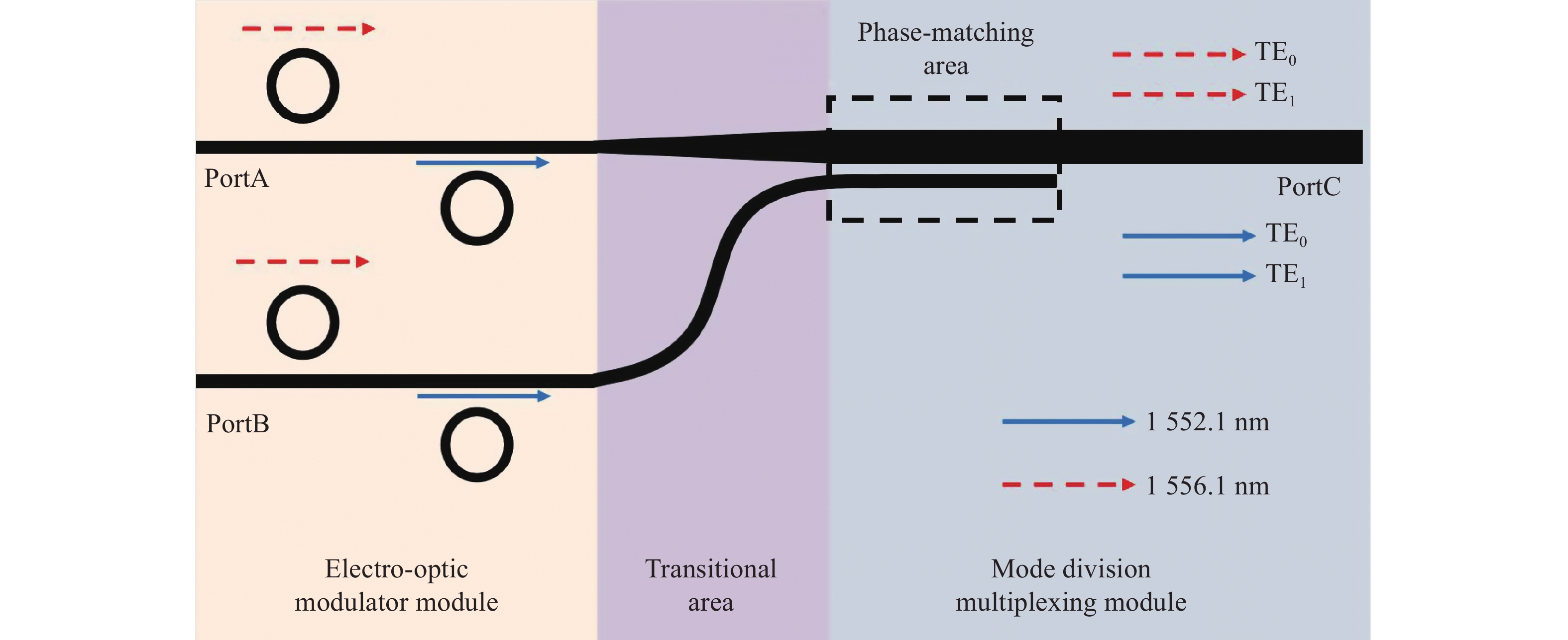
文中所提出的双波长电光调制器和模分复用集成器件主要由两个模块组成,分别是光子晶体电光调制模块和非对称定向耦合型模分复用模块,它的理论模型如图1所示。该集成器件的电光调制模块采用的L3型复合谐振腔(标记为圆圈)的设计,即将两个L3腔呈斜对角式分布在光子晶体波导两侧,通过微调两个L3腔周围的空气孔,分别实现对1552.1 nm和1556.1 nm光波的“通”“断”状态调制。模分复用模块采用硅基非对称平行纳米线波导结构,通过施加不同的电压,可以在波长 1552.1 nm和1556.1 nm处实现TE0、TE1的复用功能。为了减少光子晶体波导和纳米线波导之间的级联损耗,在其连接处采用锥形波导过渡。未施加电压时,当入射光波与调制模块的L3腔的谐振波长匹配时,入射光波会被局域在L3谐振腔内,实现调制器的“断”状态。相反, 当施加电压时,入射光波与调制模块的L3腔的谐振波长失配时,入射光将不会被局域在谐振腔内,而是沿着光子晶体波导进入模分复用模块,实现调制器的“通”状态。从端口A、B经调制后的TE0模进入单模波导中传输,会在相位匹配区发生模式转换,端口B的TE0模将转换为TE1模并耦合至双模波导中,与端口A的TE0模同时从端口C输出,实现两个模式的复用。

Figure 1. Theoretical model of dual-wavelength electro-optic modulator and mode division multiplexing integrated device
-
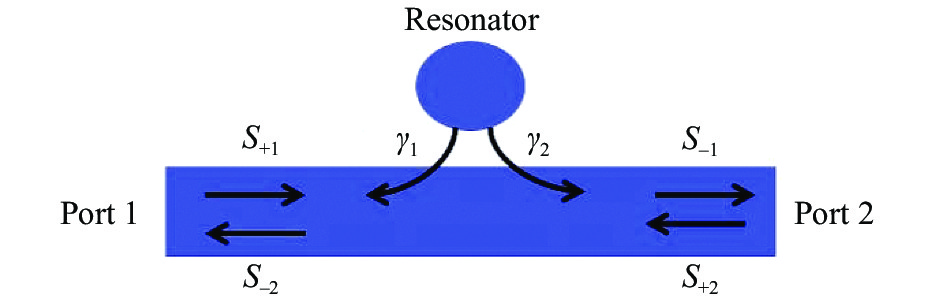
电光调制模块是在光子晶体平板中引入两个L3型谐振腔,通过改变空气孔半径以及平移空气孔位置,使得两个腔的谐振波长处于两个工作波长。该复合腔的两个L3腔均与光子晶体线缺陷波导构成侧耦合结构,取其中一个L3腔进行理论分析,其理论模型如图2所示。

Figure 2. Theoretical model of side coupling structure
图2中,输入与输出光波的幅值分别为
$ {S}_{+i} $ 和$ {S}_{-i} $ ,谐振腔与波导耦合过程中产生损耗时的幅值耦合衰减系数为$ {\gamma }_{i}(i=\mathrm{1,2}) $ 。由时域耦合模理论可以推导得出该模型中谐振腔的幅值变化为:式中:A为谐振腔的幅值;
$ {\omega }_{0} $ 为谐振腔的谐振频率。根据能量守恒定律和时间反演对称性得到公式(2)和(3):当光只从端口1入射时,
$ {S}_{+1}=1 $ ,$ {S}_{+2}=0 $ ,并且$\dfrac{{\rm{d}}A}{{\rm{d}}t}=-i\omega A$ 。再令$ {\gamma }_{1}={\gamma }_{2}=\gamma $ ,得到透射谱$ T\left(\omega \right) $ 的表达式公式(4):经过上述分析可知,当入射光的谐振频率与L3型谐振腔的谐振频率一致时,光波被局域在谐振腔内,端口2处的透射率可以达到最低,实现调制器的“断”状态;否则光波能量将从端口2处输出,此时透射率可以达到最高,实现调制器的“通”状态。
光子晶体谐振腔型电光调制器的工作原理是基于等离子色散效应,即载流子的注入或抽出会改变半导体材料中的自由载流子浓度,从而导致材料的有效折射率发生变化。当硅基材料的工作波长在1550 nm 附近时,硅基材料的吸收系数和折射率随着载流子浓度变化的对应关系式为[20]:
式中:
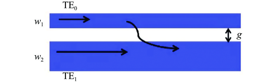
$ \Delta {N}_{e} $ 为电子浓度变化量;$ \Delta {N}_{h} $ 为空穴浓度变化量;$ \Delta {n}_{c} $ 为材料有效折射率变化量;$ \Delta {\alpha }_{c} $ 为单位长度吸收系数的变化量。由公式(5)和(6)可知,随着载流子浓度的增大,吸收系数逐渐增大,而折射率将逐渐减小。文中所设计的电光调制器便是基于此原理,在谐振腔两端加上调制电压,改变 P型和N 型载流子浓度(即空穴和电子浓度),从而使材料的有效折射率发生改变,最终使得L3型谐振腔的谐振频率发生动态偏移,改变调制器的“通”“断”状态。模分复用模块采用单模波导与多模波导耦合结构来实现模式的复用功能,其理论模型如图3所示。

Figure 3. Theoretical model of silicon-based mode division multiplexing
利用横向耦合模理论对该非对称平行波导进行研究,两个耦合模的线性微分方程为公式(7)和(8):
公式中:A1、A2分别是在单模波导和多模波导中传输的光波振幅;β1、β2分别是单模波导和多模波导中的传播常数;c是耦合系数且为常数。引入边界条件
$ {A}_{1}\left(0\right)=1,{A}_{2}\left(0\right)=0 $ ,由此可以推出光波的传输功率为:式中,P1、P2分别是单模和多模波导中传输的光功率;
$ Q=\dfrac{2 c}{\;{\beta }_{1}-{\;\beta }_{2}} $ ,当Q→∞即$\; {\beta }_{1}=\;{\beta }_{2} $ 时,波导中的光振幅可表示为:由上式可知,当
$ {\;\beta }_{1}={\beta }_{2} $ 时,单模波导中传输的光功率与多模波导中传输的光功率完全耦合。根据横向耦合模理论,模式转换的本质为有效折射率的匹配,即[18]:经过上述分析可知,在该模块中,为了实现最佳耦合,需要满足光波在单模波导和多模波导中传播常数相等,即TE0和TE1模式所对应的有效折射率相等。
-
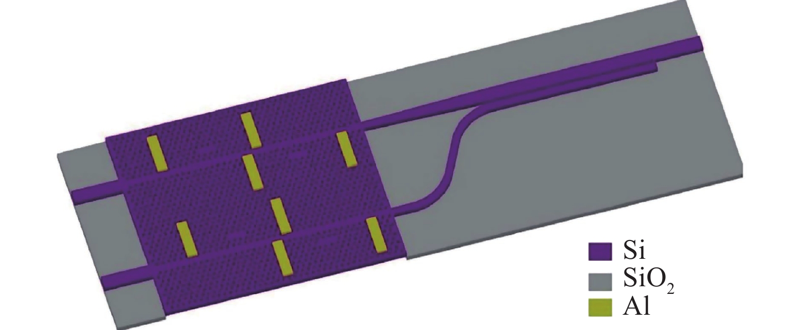
基于光子晶体的双波长电光调制和模分复用的集成器件的三维结构如图4所示。它由两部分组成,包含三角晶格圆形空气孔型的光子晶体平板和硅基纳米线波导。光子晶体平板部分为空气桥结构,即平板上下包层为空气。纳米线波导的衬底材料为二氧化硅,其对应的折射率为1.4。

Figure 4. Three-dimensional structure of integrated device of photonic crystal dual-wavelength electro-optic modulation and mode division multiplexing
光子晶体平板和纳米线波导的材料均为硅,其折射率为3.47。为了方便器件级联,提高集成器件的兼容性,光子晶体平板的厚度和硅基纳米线波导的厚度一样,均采用220 nm。在L3腔的两侧分别加电极(图中标记为Al),左侧为正极、右侧为负极。以下分别对电光调制模块和模分复用模块进行单独的结构设计与优化。
-
文中设计的双波长电光调试器采用两个L3型谐振腔,其结构如图5(a)所示。L3腔是在光子晶体平板中的某一行去除三个空气孔而形成的腔结构,可以形成良好的光子局域。为了减少两个腔之间的相互影响,将两个腔呈斜对角式分布在光子晶体波导两侧。此时,两个L3 腔与光子晶体波导的耦合方式均为侧耦合,相当于一个带阻滤波器。光子晶体的晶格常数
$ a=0.4\;{\text{μm}} $ ,空气孔半径为$ r=0.096\;{\text{μm}} $ 。为了增强微腔的局域效果,对A、B两个L3腔进行了优化设计。以A腔优化为例, 图5(b)为L3腔谐振波长和透过率随黄色空气孔半径R变化图,图5(c)为L3腔谐振波长和透过率随腔上下8个空气孔内移距离Δd的变化图。从中可以发现,黄色空气孔半径R减小,谐振波长右移,反射率增大;空气孔内移的距离Δd减小,谐振波长右移,反射率增大。当R=84 nm, Δd=40 nm时,A腔实现了对1556.1 nm的光调制。同理,通过优化B腔的参数,实现了对1552.1 nm的光调制。 
Figure 5. (a) Structure diagram of electro-optic modulation module; (b) Variation of the resonance wavelength and transmittance of the L3 resonator with the radius R of the yellow air hole; (c) Variation of the resonance wavelength and transmittance of the L3 resonator with the moving distance Δd of the upper and lower air holes
优化后的L3腔上下8个空气孔向内移动0.1a,左右两个黄色空气孔向外移动0.2a,左右两个绿色空气孔向外移动0.1a。同时,为了实现对两个波长的调制,优化空气孔的半径,A腔上下8个空气孔半径为
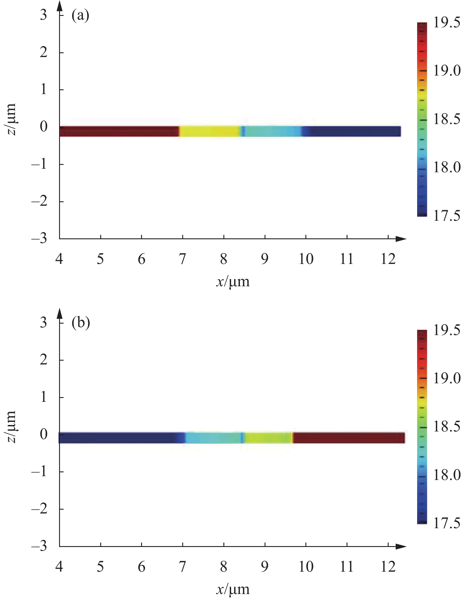
$ 0.092\;{\text{μm}} $ ,黄色空气孔半径为$ 0.084\;{\text{μm}} $ ,绿色空气孔半径不变,B腔上面4个空气孔半径为$ 0.092\;{\text{μm}} $ ,下面4个空气孔半径不变,黄色空气孔半径为$ 0.076\;{\text{μm}} $ ,绿色空气孔半径不变。调制器模块的电学掺杂结构如图6所示,由于B腔与A腔结构相似,此处以A腔掺杂为例。在L3腔左右两侧加电极(左侧接正极,右侧接负极),采用竖直掺杂形成PN结,PN结的掺杂浓度为 P+=5.4×1019 cm−3, N+= 4.8×1019 cm−3,P=3.9×1018 cm−3,N= 2.8×1018 cm−3。使用Lumerical中的Device模块进行分析,当驱动定压为1.05 V时,电子浓度变化量ΔNe = 2.21×1018 cm−3,空穴浓度的变化量ΔNh = 3.51×1018 cm−3(如图7所示)。根据公式(5)可以得到此时硅基平板的折射率变化量可以达到0.008,实现对1556.1 nm波长的“通”状态调制。对B腔采用同样的掺杂结构,可以实现对1552.1 nm波长的“通”状态调制。图8是3D-FDTD仿真得到的透射谱图,从图中可以看出,当不施加电压时,该调制器对1552.1 nm和1556.1 nm的光透过率趋近于零,此时相当于电光调制器的“断”状态;当A腔、B腔同时施加电压时,两个谐振波长同时发生偏移,原谐振波长处的透射率升高,可以使1552.1 nm和1556.1 nm的光波同时通过调制器,如图8(a)所示;当A腔不施加电压、B腔施加电压时,可以使1552.1 nm的光波通过调制器,如图8(b)所示;当A腔施加电压、B腔不施加电压时,可以使1556.1 nm的光波通过调制器,如图8(c)所示。从而实现对两个波长的通断调制。

Figure 6. Schematic diagram of electro-optic modulator doping structure

Figure 7. Carrier concentration distribution diagram when the voltage across both ends is 1.05 V. (a) P-type carrier concentration; (b) N-type carrier concentration

Figure 8. Transmittance diagram of output port 2 when voltage is applied to different resonators.(a) Voltage is applied to both resonators A and B; (b) Only the voltage is applied to the B resonator; (c) Only the voltage is applied to the A resonator
-
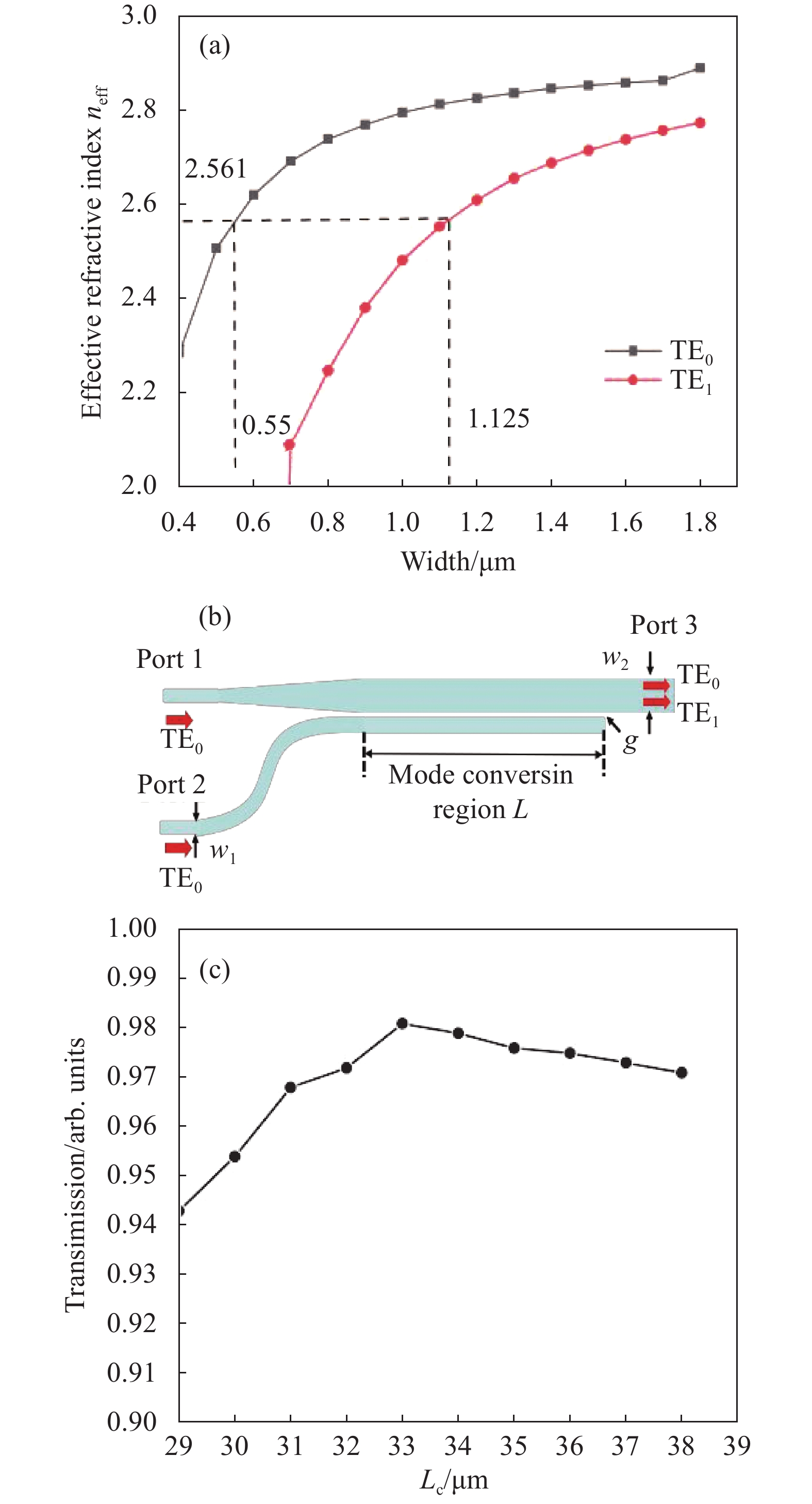
模分复用模块采用非对称定向耦合型结构,当工作波长为1540~1560 nm时,包层为二氧化硅的硅基纳米线波导TE0和TE1的有效折射率如图9(a)所示。由图9(a)中的曲线可以看出,当单模波导宽度w1=0.55 μm、多模波导宽度w2=1.125 μm时,TE0和TE1的有效折射率均为2.561。此时,满足模式匹配条件,实现模式转换。

Figure 9. (a) Effective refractive index map of nanowire waveguide; (b) Structure diagram of mode-division-multiplexing module; (c) Relationship between different coupling lengths and coupling efficiency
基于模式匹配原理,设计的模分复用模块结构如图9(b)所示。当特定波长的TE0模式光波从Port 1输入时,仍以TE0模式光波在双模波导中传输。当特定波长的TE0模式光波从Port 2输入到单模波导中,经过长度为L的模式转换区,会从单模波导耦合至双模波导中,并转换为TE1模式。最终,在Port 3处输出TE0和TE1两个模式的光波,实现TE0和TE1两模式的模分复用功能。
在此基础上,将探测器放置在输出端口3,选取波导间距g=0.1 μm,调节耦合长度Lc,使耦合效率达到最高。1554 nm中心波长下不同耦合长度Lc与耦合效率即透过率的关系如图9(c)所示,当Lc=33 μm时,波导w1中TE0模式耦合到波导w2中的效率最高,达到0.981。
-
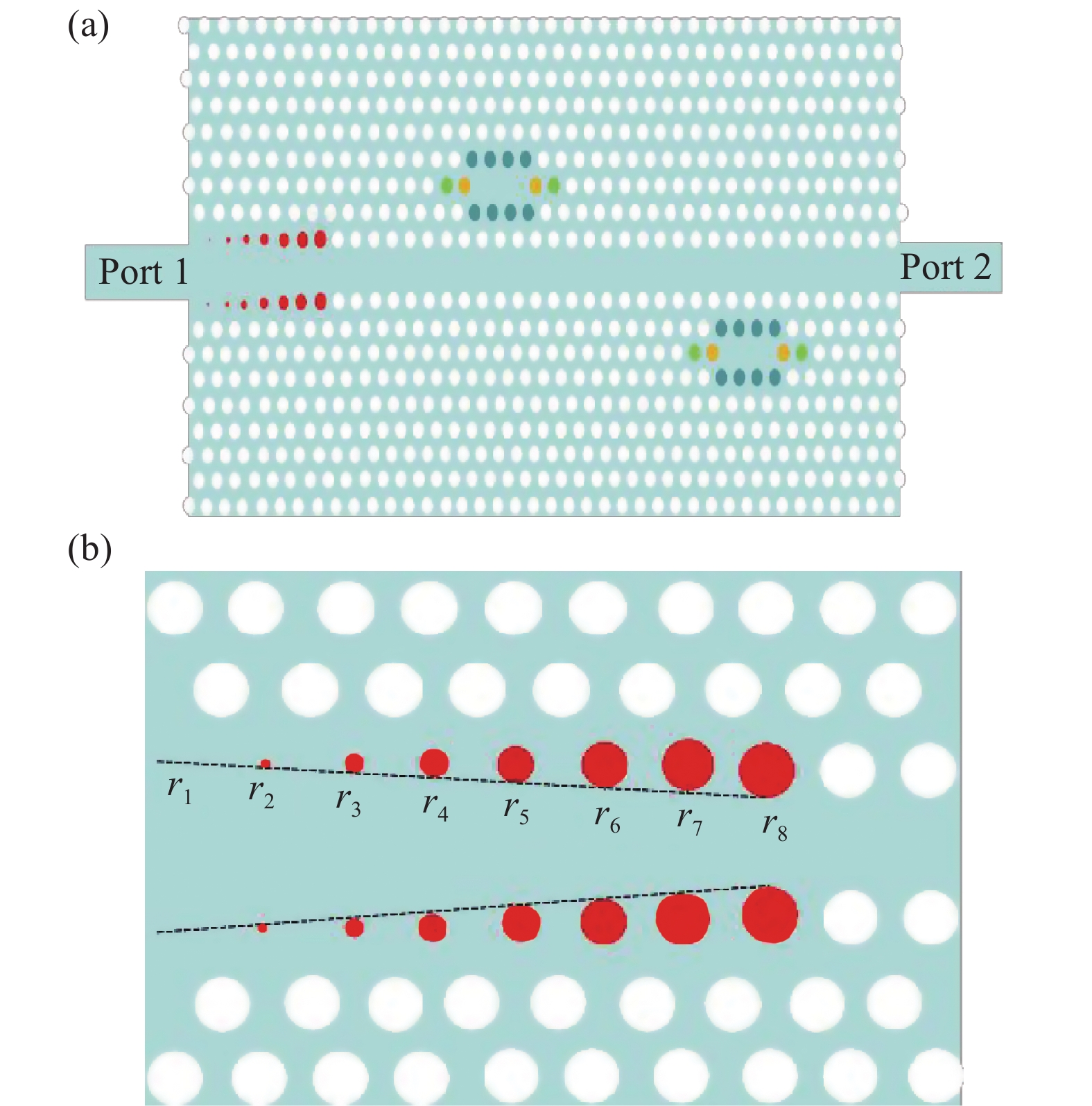
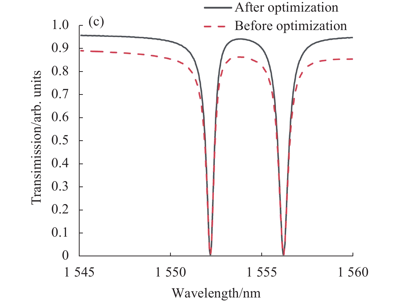
由于输入端线波导的导光机制是全内反射效应,光子晶体平板线缺陷波导的导光机制是禁带效应,二者的导光机制不同,所以它们各自的传播常数不同,即波导的有效折射率不同。因此,二者在级联时会出现模式失配的情况,从而产生大量散射损耗。为了减少级联损耗,提高透过率,在输入端口级联处引入锥形空气孔结构,如图10(a)中红色空气孔部分所示。图10(b)是锥形结果具体参数示意图,其中,红色空气孔的半径
$ {r}_{n}=\dfrac{r}{c}\left(n-1\right) $ 且n≤c+1,r为光子晶体空气孔的半径,c为锥形结构其中一侧红色空气孔的个数,n为锥形结构其中一侧红色空气孔的序号。当c=7时,电光调制器的透射效果最优[19]。此时,第一个空气孔(n=1)的半径$ {r}_{1}=0\;{\text{μm}} $ ;第二个空气孔(n=2)的半径$ {r}_{2}=0.014\;{\text{μm}} $ ;以此类推,直到n=8时,$ {r}_{8}=r= 0.096\;{\text{μm}} $ ,即最后一个空气孔和光子晶体空气孔半径相等。图10(c)分别是引入锥形空气孔结构前后调制器“通”状态下,光从端口1输入从端口2输出的透射率图,从图中可以看出,光在输出端口2的透射率提升了9%左右。因此,在级联器件的输入端引入锥形空气孔结构,以提高透射率。

Figure 10. (a) Schematic diagram of the modulation module structure after cascading; (b) Schematic diagram of cone structure; (c) Input the transmission spectrum before and after optimization of the waveguide
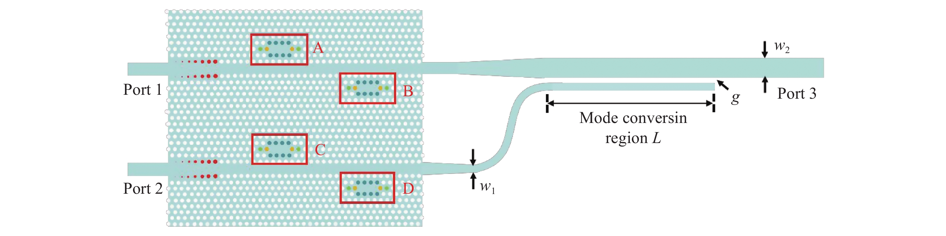
图11是双波长电光调制器和模分复用器级联的结构图。由于级联后,L3谐振腔的谐振波长会出现偏移,为了使集成器件的调制波长与单独调制的波长一致,通过微调A、B、C、D四个谐振腔中黄色空气孔的半径,将谐振波长移到1552.1 nm和1556.1 nm。级联微调之后,A、B、C、D四个谐振腔黄色空气孔的半径分别为0.083、0.091、0.086、0.083 μm,可以实现中心波长为1552.1 nm和1556.1 nm的TE0模、TE1模通断调制及两模式模分复用功能。该集成器件结构紧凑,尺寸约为65 μm×18 μm。

Figure 11. Overall integrated device structure diagram
-
文中所设计的双波长电光调制与模分复用集成器件,需要考虑的性能指标主要有消光比、插入损耗、调制速率、调制深度和信道串扰。
消光比定义为:
式中:Imax和Imin分别是调制器在“通”和“断”状态下对应的输出光强。消光比的单位是dB,消光比越大,调制性能越好。
插入损耗定义为:
式中:Iout和Iin分别是调制器的输出光强和输入光强。插入损耗的单位是dB,插入损耗越小,调制性能越好。
调制速率是指调制设备单位时间可调制的码元速率,在电光调制器中能反应“通”、“断”调制的转换速度,其与集成器件的系统总响应时间T成反比,其表达式如下:
式中:
$ {t}_{re} $ 为材料的响应时间;$ {t}_{s} $ 为器件的稳定时间。调制速率的单位为GHz,调制速率越大,调制性能越好。调制深度定义为:
式中:P1和P2分别是调制器在“通”和“断”状态下对应的输出光功率。调制深度越大,表示调制器越有利于长距离、低误码率传输,调制效果越好。
信道串扰定义为:
其中,
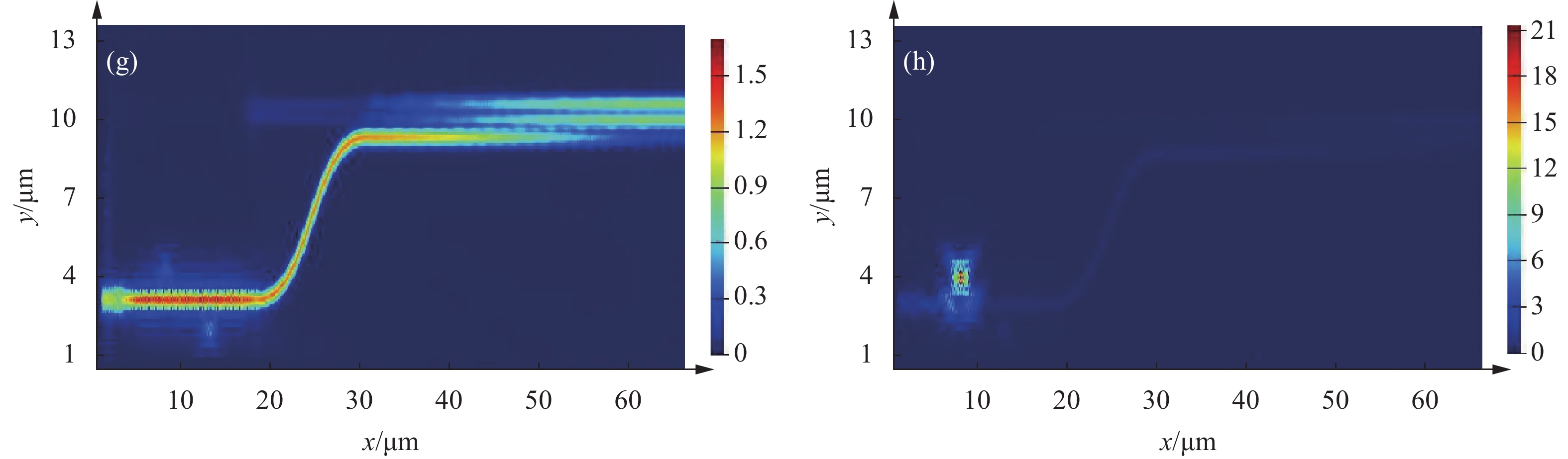
${I}_{{\rm{out}}}$ 和${I}'_{{\rm{out}}}$ 分别为集成器件目标输出端口与非目标输出端口的光强。信道串扰的单位是dB,信道串扰越小,调制性能越好。采用Lumerical仿真软件中的时域有限差分法(3D-FDTD)分析了集成器件的消光比、插入损耗、调制电压、调制速率、调制深度和信道串扰值。仿真计算时,光源分别放置在输入端口1和2,探测器放置在输出端口3,图12(a)~(h)分别为波长1552.1 nm和1556.1 nm下TE0和TE1“通”、“断”状态的稳态场分布。


Figure 12. On-off steady-state field distribution diagrams of different wavelengths and modes. (a) 1552.1 nm TE0 "on" state; (b) 1552.1 nm TE0 "off" state; (c) 1552.1 nm TE1 "on" state; (d) 1552.1 nm TE1 "off" state; (e) 1556.1 nm TE0 "on" state; (f) 1556.1 nm TE0 "off" state; (g) 1556.1 nm TE1 "on" state; (h) 1556.1 nm TE1 "off" state
当该集成器件分别处于“通”和“断”状态下时,利用3 D-FDTD进行仿真,得到对应的稳定时间,如图13所示。由于器件的调制响应时间应以“通”状态至“断”状态、“断”状态至“通”状态中的较大值为准[20],因此选取“通”状态下的稳定时间约为27 ps。当电压为0~2 V时,硅在电场控制下的材料响应时间为30 ps[20],所以该集成器件的系统响应时间为57 ps。通过公式(16)和公式(17),得到器件的调制速率为17.54 GHz。通过公式(14)和(18)计算得到该器件的消光比ηER均为20 dB以上,调制深度D均为0.99。通过公式(15)和(19)可得:该集成器件的插入损耗γIL最小为0.47 dB,最大为0.57 dB;信道串扰值C CT最小为−39.50 dB,最大为−34.68 dB。表1对比了参考文献所提出的同类型器件,文中所设计的集成器件可以调制两个波长两个模式四个信道,在保证器件小型化的前提下,扩充了信道数,增加了传输容量。并且从表1中可以看出,该集成器件消光比高,信道串扰低且结构紧凑,易于集成。

Figure 13. Stable time when the integrated device is in the "on" and "off" states. (a) "on" state; (b) "off" state
Reference Extinction ratio/dB Insertion loss/dB Channel crosstalk/dB Footprint [8] - 4-5 - 200 μm [9] 15.1 0.3 - 46 μm×8 μm×0.22 μm [10] 3-4 1 - 200 μm [11] 29.13 1.33 - 9.03 μm [12] - 0.3 <−36 300 μm [13] - 0.3 <−22 >48.8 μm [14] - <1.5 <−30 >100 μm [15] - <3.2 <−21 18 μm [17] 13-16 22 - 0.45 mm2 [18] 19.73 <0.46 <−14.66 54 μm×22 μm This work >21.65 <0.57 <−34.68 65 μm×18 μm Table 1. Performance comparison of photonic crystal electro-optic modulator and two-mode mode division multiplexing integrated device
-
文中提出了一种基于光子晶体的双波长电光调制和模分复用的片上集成器件,采用L3型复合谐振腔和硅基光子晶体波导侧耦合结构,通过调节谐振腔的宽度和空气孔的半径,可以实现两个波长的调制和模分复用功能。在纳米线波导与光子晶体波导之间引入锥形空气孔结构来减少耦合损耗,提高透射率。采用PN结掺杂结构可以在较小的折射率差的条件下实现较低的调制电压。仿真结果表明,该集成器件在调制电压为1.05 V时,实现中心波长为1552.1 nm和1556.1 nm的TE0模、TE1模通断调制及复用功能,其消光比高,调制深度大,信道串扰低且结构紧凑,易于集成,可望应用于高速大容量光通信系统,对集成光学器件的发展具有重要价值。
Integrated device of dual-wavelength electro-optic modulating and mode-division multiplexing based on photonic crystal
doi: 10.3788/IRLA20211107
- Received Date: 2021-12-27
- Rev Recd Date: 2022-02-09
- Available Online: 2022-11-02
- Publish Date: 2022-10-28
-
Key words:
- photonic crystal /
- dual-wavelength modulation /
- finite-difference time-domain method /
- mode-division multiplexing /
- L3 composite resonator
Abstract: In order to realize the miniaturization and multi-function of optoelectronic devices and further improve the capacity and speed of information transmission, an on-chip integrated device based on photonic crystal for dual-wavelength electro-optic modulation and mode division multiplexing (MDM) is proposed. The electro-optical modulation module of the integrated device is composed of a silicon-based photonic crystal waveguide and two L3 composite resonators, and the MDM module consists of silicon-based asymmetric parallel nanowire waveguides. A silicon-based photonic crystal waveguide is used at the junction of the two modules. The L3 composite resonators and PN doping structure are used to achieve the modulation of the two-wavelength TE0 mode, and the asymmetric directional coupling structure is used to convert the TE0 mode of two wavelengths into the TE1 mode. The parameters of the integrated device are calculated using three-dimensional finite-difference time-domain (3D-FDTD) method. The results show that when the voltage is 1.05 V, the integrated device can achieve a center wavelength of 1 552.1 nm and 1 556.1 nm TE0 mode, TE1 mode on-off modulation and two-mode mode division multiplexing function. The extinction ratio of the device is as high as 24.67 dB, and the modulation depths are both 0.99. The insertion loss and the channel crosstalk are less than 0.57 dB and −34.68 dB, respectively. And the minimum modulation speed is 17.54 GHz. The integrated device has compact structure and is expected to be applied to high-speed and large-capacity optical communication systems.


 DownLoad: