


-
在利用光谱技术进行目标探测识别的光电系统中,为了实现对目标的精准有效探测,窄带滤光片作为一个重要的光学元件被广泛应用[1-3]。该类窄带滤光片能够提高目标与背景的信噪比,从而提高对目标信号的提取效率与正确率。随着目标探测识别向着多波段调谐探测方向的发展,多通道窄带滤光片的应用也愈发频繁,其应用能够有效地缩小探测系统的体积与重量,增加探测通道数量,已成为探测识别系统的发展与研究方向之一[4-5]。
多通道滤光片是通过改变间隔层的物理厚度来调控不同通道的峰值波长,因此制备多通道滤光片的关键在于制备不同物理厚度的间隔层,其主要制备方法有组合镀膜、组合套刻、拼接集成 [6-9],但这些方法均存在自身的局限性。Yingbu Duan等人采用组合镀膜制备了应用于中波红外6通道的窄带滤光片,该方法以“增材”的方式通过控制薄膜沉积区域得到各通道间隔层厚度,在多次套镀过程中需严格控制工艺一致性,对掩模精度及工艺稳定性要求较高,因此成品率低、制备周期长[6]。罗海瀚等人采用多个掩膜版组合套刻工艺,此方法与组合镀膜法类似,以“减材”的方式在一定厚度的间隔层材料上通过刻蚀得到各通道间隔层厚度,同样对掩模精度及工艺稳定具有高要求,而且成品率低及制备周期长[7]。李得天等人采用拼接集成的方式制备了4通道红外滤光片,根据各通道的光谱需求,分别制备出符合需求的单通道滤光片,将各通道通过胶合的方式集成至空白基片上,从而得到多通道滤光片[8]。此方法可应用于通道数较少的多通道滤光片制备,对于高集成度、小尺寸的需求,此法较为乏力。为了解决这些问题,笔者提出采用纳米压印技术制备阵列结构多通道滤光片的间隔层。该技术具有效率高、成本低等优点,已经得到了广泛的应用。2016年,刘鑫等人采用纳米压印技术,对衍射光学元件进行了加工,实现了该类元件的高保真、低成本、批量化制备[10]。2017年,褚金奎等人采用柔性纳米压印技术制备了中红外双层金属纳米光栅,得到了优异的消光比特性与偏振特性[11]。2019年,葛少博等人利用纳米压印与电感耦合等离子体刻蚀技术,制备了轮廓渐变的薄膜微金字塔结构阵列,实现了结构单元尺寸1.5~10 μm之间的调控[12]。
纳米压印技术通过图形转移,将模具的图形转移到间隔层薄膜上,一次统一调整多个通道的间隔层厚度,实现间隔层厚度的精确调整,保证了工艺一致性,实现中心波长精准控制。其中的模具制作尤为重要,而多通道滤光片间隔层的物理结构分布决定了模具图形的结构。文中主要研究阵列结构多通道滤光片间隔层模具的制备方法,提出基于单点金刚石车削(Single Point Diamond Turning, SPDT)的快刀伺服技术(Fast Tool Servo, FTS)对其进行加工,利用白光干涉(White Light Interference, WLI)与拼接测量技术对其表面形貌进行检测,进而评价该模具的制造精度。针对5×5阵列结构多通道滤光片的设计要求,完成了对应硬模具的制造,其精度满足应用要求。
-
基于F-P结构的窄带多通道滤光片是通过改变间隔层物理厚度来调节不同通道的峰值波长,使其透过率达到最大。针对波长在650~740 nm范围内,半宽度为10 nm的10通道窄带滤光片,选用G|(LH)5(4L)(HL)5 |A为基础膜系,L为低折射率材料,选用SiO2,H为高折射率材料,选用H4。在TFCalc软件中进行优化设计,得到中心波长700 nm处的最大透过率为95.7%,截止透过率为2.2%,峰值半宽度(FWHM)为10 nm。TFCalc中优化得到的间隔层4L的物理厚度如表1所示。
Wavelength/nm 650 660 670 680 690 700 710 720 730 740 Thickness of spacer-layer (4L)/nm 401.6 431.6 446.6 461.6 476.6 491.6 506.6 531.6 546.6 561.6 Table 1. Physical thickness of the spacer-layer at 650-740 nm after optimized
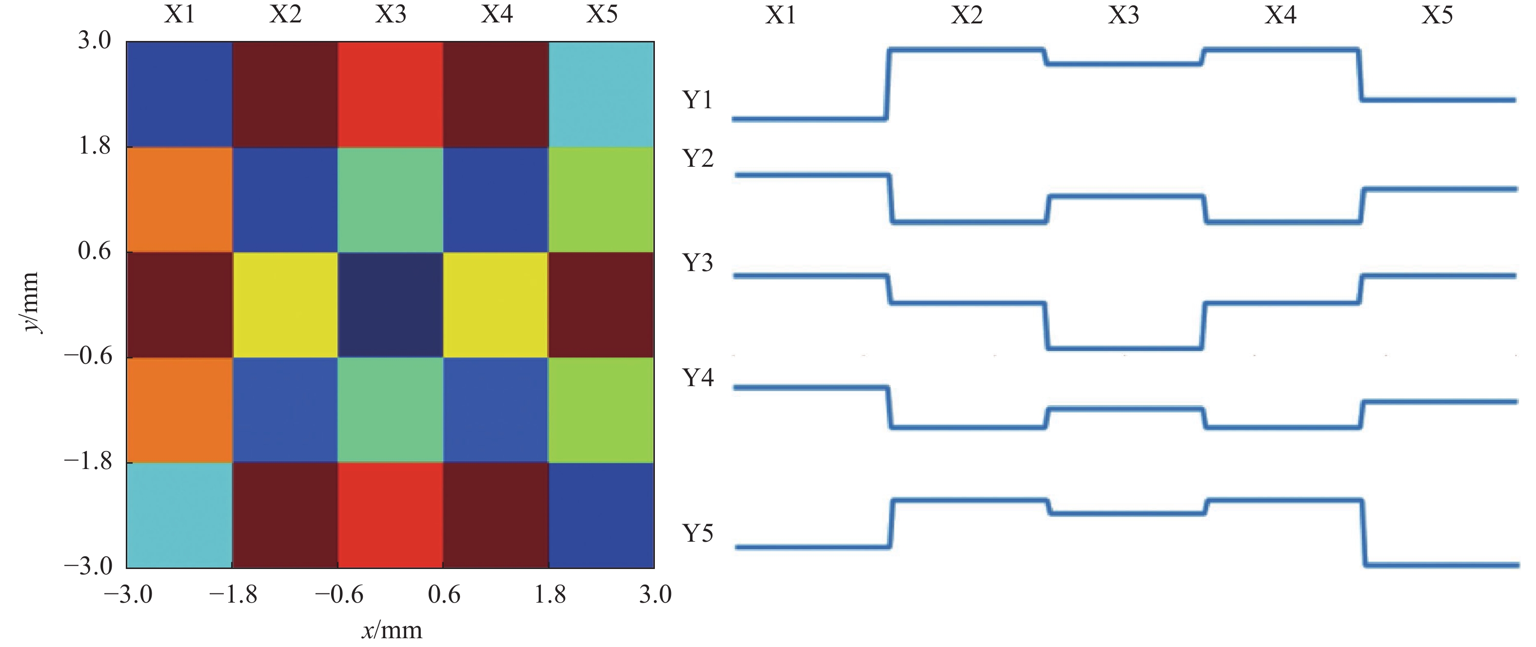
表1中,选取波长650 nm对应的401.6 nm间隔层物理厚度为参考平面,则相应的物理厚度差分别为0、30、45、60 、75、90、105、130、145、160 nm。采用纳米压印的方式对该多通道滤光片的间隔层物理厚度进行调控,需要不同物理厚度的模具。多通道滤光片中的所有厚度均为正值,故对应到其模具上,这些值应为负值(表示为参考平面向下的高度值)。将这些通道按照5×5阵列方式放置,为了减少加工难度,同时考虑压印过程中的胶材料气泡排除情况,将相邻通道按台阶高度差最大化原则进行排布,排列如表2所示。
Channel number X1 X2 X3 X4 X5 Y1 −145 0 −30 0 −105 Y2 −45 −145 −90 −145 −75 Y3 0 −60 −160 −60 0 Y4 −45 −130 −90 −130 −75 Y5 −105 0 −30 0 −145 Table 2. Physical thickness distribution of 5×5 array multi-channel filter spacer-layer mold (Channel size 1.2 mm×1.2 mm, thickness unit: nm)
根据表2中的模具物理厚度数据,及其单个通道(横向尺寸)的尺寸为1.2 mm×1.2 mm,在MATLAB中仿真得到该多通道滤光片模具的二维结构图与三维分布情况。如图1所示,该模具为方形台阶结构,横向尺寸相同,纵向尺寸为纳米量级,且排布几乎无规律,因此普通的方法难以加工。

Figure 1. Simulation of 5×5 multi-channel filters spacer-layer mold
-
由图1(b)可以看出,该模具的纵向高度分布几乎是“杂乱无章”的,常规的模具加工方法难以实现。文中提出采用FTS的加工方式,利用该系统纳米量级的位置精度伺服控制能力与强大的加速度控制能力(能实现高频运动),对模具进行加工。
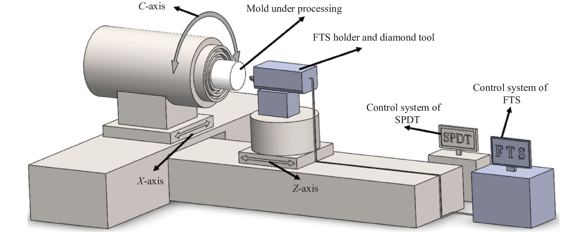
FTS工作原理如图2所示,机床结构以 T 型布局为基础,在主轴轴向方向上附加一套快速精密的进刀装置。工件安装在主轴上,并随主轴做旋转运动,通过精密监测极坐标值(半径X,角度C),精确控制Z轴的位置;金刚石刀具安装在快刀刀架的前端,FTS系统通过单点金刚石车床运动中的极坐标值(半径X,角度C),实时驱动金刚石刀具进行高频直线运动,从而在模具表面加工出所需的纵向高度信息[13-15]。

Figure 2. Schematic diagram of FTS
由于模具随主轴进行旋转运动,故金刚石刀具在模具表面的加工轨迹为螺旋线轨迹。FTS系统进刀量由模具表面的高度信息控制,如图3所示。
由图3可知,图(b)仿真了当加工半径为2.8 mm时,刀具在该半径的360°内进刀量的分布情况。在FTS系统中,进刀量为负数表示刀具相对于零点位置进刀多少,为正数表示刀具相对于零点位置退刀多少。如图中,当加工半径为2.8 mm,加工角度为150°时,进刀量Z为−45 nm,表示此时金刚石刀具相对于零点位置进刀45 nm。

Figure 3. Simulation results of machining track on mold surface
-
虽然多通道滤光片间隔层模具的纵向高度分布是无规律的,但其高度差并不大,仅为百纳米量级。因此,可采用WLI测量技术对模具的表面形貌进行测量,但由于WLI的测量视场有限,而5×5多通道滤光片的横向尺寸为6 mm×6 mm,远大于WLI的测量视场。故需采用拼接测量的方式,拓展测量区域,测量更大区域的表面形貌,如图4所示。
从图可以看出,拼接测量时,按照1,2,···的顺序,依次测量,然后通过拼接数据处理,即可获得整个测量区域的表面形貌[16-17]。因此,在两次相邻测量中,必须有重叠区域,便于数据处理过程中的拼接计算。测量次数与单次测量区域的大小、重叠区域的重叠率,以及需要测量表面的整体尺寸有关。由于拼接测量技术的测量次数较多,该技术所需的测量时间较长。

Figure 4. Schematic diagram of stitching measurement technique
由于白光测量技术具有亚纳米量级的纵向测量精度和微米量级的横向测量精度,故测量得到模具表面的形貌分布能够真实反映该模具的加工精度,即可用该测量结果对加工精度进行评价分析。对多光谱滤光片模具而言,除了关心模具表面单个通道的平整度精度外,更关心模具的尺寸结构加工精度。由于该模具属于台阶结构,在分析其尺寸结构精度时,将该5×5结构的某一行的5个通道的设计曲线与实际测量结果中对应5个通道的测量曲线进行比较,分析得到其横向尺寸和纵向尺寸的加工精度分布情况。其各个通道的理论设计曲线如图5所示。

Figure 5. Vertical height distribution curve of Y1-Y5 channels
-
结合实验室情况,针对如图1所示的多通道滤光片间隔层模具,在保证加工表面质量和纳米压印要求的情况下,选用的基底材料为单晶锗。其中,单点金刚石车床为Precitech 公司的Nanoform 700 Ultra,FTS系统也为该公司的FTS500,即相对于该刀架的零点位置,可进刀和退刀的行程各为250 μm,其最大行程为500 μm。该快刀系统的最大进刀频率为1000 Hz,加速度为20 g。同时,加工过程中所用的金刚石刀具参数与加工参数如表3所示。表中所示的切削深度为800 nm,是指单点金刚石车床Z轴的进给深度,而FTS系统的进给变化范围为160 nm,与表2中该模具的厚度变化范围保持一致。
Parameters of diamond tool Value Parameters of processing Value Tool radius/mm 0.234 Spindle speed/r·min−1 400 Rake angle/(°) −25 Feed rate/mm·min−1 0.5 Conic clearance/(°) 10 Cutting depth/nm 800 Waveness/nm ≤250 Table 3. Diamond tool parameters and cutting pro-cessing parameters

Figure 6. Processing and detection site for the spacer-layer mold of multi-channel filter
FTS加工方式在生成加工数据时,工件表面的取点方式有等角度取点和等弧长取点两种方式[14],由于该模具表面为方形台阶型结构(非连续结构),为了减小各台阶边缘过渡区域对模具的影响,应选用等弧长取点方式,如图3(a)所示。采用该方式,同时,使用的金刚石刀具半径Rtool为0.234 mm,加工得到的模具表面各通道间的台阶边缘过渡最大横向尺寸约110 μm,满足设计过渡区域小于200 μm的要求。
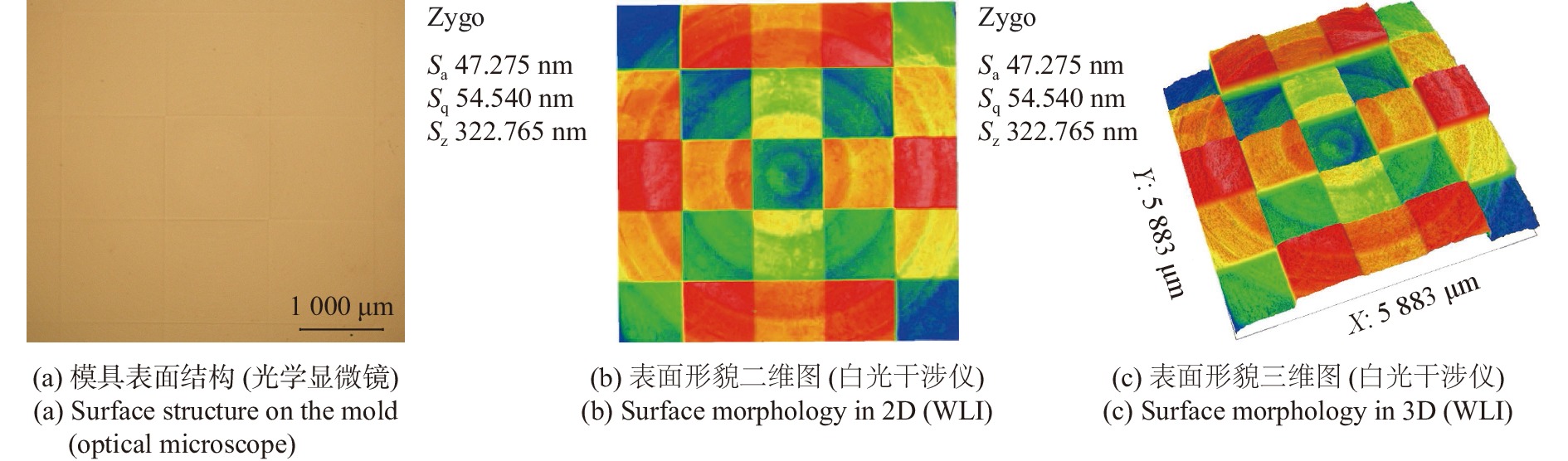
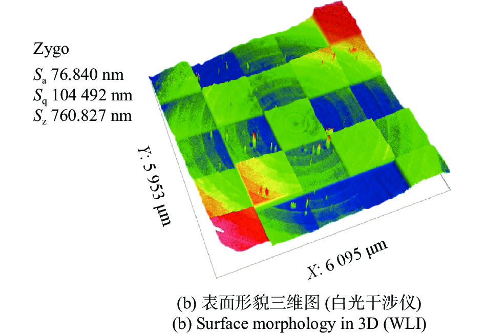
加工完成后,采用实验室的Zygo NewView 8200WLI对模具表面进形貌行测量(图6(a)),同时采用10×的Mirau物镜,场镜为1×,对应的单次测量视场为0.83 mm×0.83 mm。5×5多通道滤光片的横向尺寸为6 mm×6 mm,当设置重叠区域的重叠率为20%时,对应的测量次数至少需要81次(考虑到测量边缘拓展和留边问题,实际测量为100次)。测量完成后,设备自带的Metropro X软件能够自动拼接得到整个区域的表面形貌,如图7所示。

Figure 7. Masurement results of mold surface topography
-
对比模具表面理论数据仿真结果(图1)与模具表面形貌检测结果(图7),其横向都是方块形分布,纵向均为台阶形分布,两者具有良好的统一性。在评价多通道滤光片模具的制造精度时,采用1.3节所述的方法,需对每行5个通道的结构尺寸进行比较,读取图7中每行5个通道的台阶高度分布曲线,与图5中Y1~Y5行的通道理论曲线进行比较,其对比结果如图8所示。
图8分别对比了Y1~Y5这5行中,每行的5个通道的实验测量曲线与理论设计曲线的匹配情况。从这5幅图的对比结果可以看出,各个通道的横向尺寸方向与设计值(1.2 mm)几乎完全重合;而纵向尺寸方向,由于模具表面车削加工痕迹与粗糙度问题(如图7所示),在局部区域存在一些起伏,但总体吻合良好,达到了使用的需求。通过局部采样与直线拟合对比可以得到如表4所示的横向尺寸与纵向尺寸的误差情况。由表4可知,加工得到的5×5型多通道滤光片模具的横向尺寸相对误差优于2%,纵向台阶差相对误差优于5%。


Figure 8. Comparison of measured curves and theoretical curves for each channel in line Y1-Y5
Comparison of horizontal size sampling Comparison of vertical size sampling Design value/mm Measured value/mm Relative error Difference of step height/nm Measured value/nm Relative error 1.2 1.213 1.12% 145 147.287 1.58% 1.2 1.221 1.80% 55 56.720 3.12% 1.2 1.220 1.69% 100 101.610 1.61% 1.2 1.220 1.69% 40 41.918 4.79% Table 4. Mold structure dimension error
-
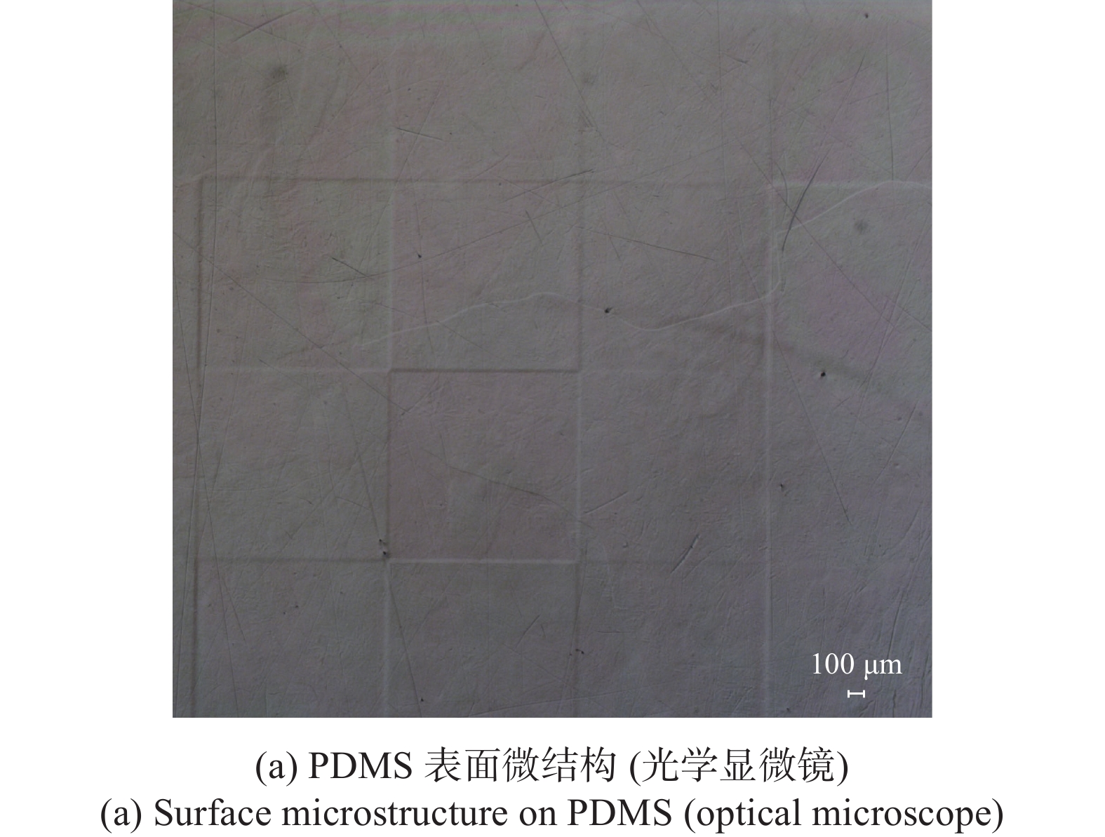
为了便于脱模,需将该模具的图形转移到软模板上。软模板的材料选用聚二甲基硅氧烷 (Polydimethylsiloxane,PDMS),这是一种直链型硅油,具有性能稳定、表面张力低、抗压缩率高的特点。采用纳米压印工艺,选用石英平板玻璃作为基底,在其上面利用PDMS将模具的图形进行转移,通过控制压印温度和时间,优化相应的压印工艺,保证图形转移的精度[18]。
图9为FTS加工的模具通过纳米压印工艺转移到PDMS上的微结构图形。通过对比PDMS的WLI检测结果(图9(b))和模具的WLI检测结果(图7(c))可以看出,它们的横向方向尺寸保持一致,纵向方向尺寸也保持了良好的“凹凸”对应关系。利用该PDMS,通过二次图形转移,即可完成阵列结构多通道滤光片间隔层的制备[18]。


Figure 9. Array microstructure graphics on PDMS
-
文中对采用纳米压印法制作阵列结构多通道滤光片的间隔层模具的加工工艺进行了分析与研究,根据5×5型多通道滤光片设计结果,对其模具进行了仿真,生成了模具表面的结构,能直观地反映该模具的通道大小以及各通道的台阶高度分布情况。根据模具的表面结构情况,选用基于单点金刚石车床的FTS加工方式,并对其加工原理与FTS系统的进刀量进行了分析。
然后在锗材料的表面对该模具结构进行了加工,并采用WLI与拼接测量技术对加工后的模具表面形貌进行了测量。从检测结果可以看出,模具表面残留一定的车削加工痕迹,这对模具表面部分区域的纵向台阶尺寸精度有一定的影响,但并不明显。通过对比测量曲线与理论曲线的情况,分析得到该模具的结构尺寸相对误差均优于5%,满足应用需求。该技术为多通道滤光片的大规模、批量化制造提供了技术支持。该制造工艺不仅能够实现多通道滤光片间隔层模具的一次性加工制造,还能为类似的非周期阵列的光学元件的快速制造提供一种有效的方法。
Manufacturing the spacer-layer mold of multi-channel filter arrays using Fast Tool Servo
doi: 10.3788/IRLA20220048
- Received Date: 2022-01-15
- Rev Recd Date: 2022-03-30
- Available Online: 2022-11-02
- Publish Date: 2022-10-28
Fund Project:
Science and Technology Department Project of Shaanxi Province(2021JM-432);Key R&D plan of Shaanxi Province(2020GY-098)
-
Key words:
- multi-channel filter array /
- spacer-layer mold /
- Fast Tool Servo /
- interference stitching measurement
Abstract: In the target detection and identification system, the signal-to-noise ratio between target and background can be improved by using multi-channel filter, so as to achieve accurate detection of target signal. The fabrication technology of multi-channel filter based on nano-imprinting has high requirements for the surface precision and structure precision of the spacer-layer mold. According to the manufacturing requirements of the spacer-layer mold of multi-channel filter array, based on the Single Point Diamond Turning (SPDT), the high-precision manufacturing of the spacer-layer mold is realized by using Fast Tool Servo (FTS). The surface morphology of the mold was detected by using White Light Interference (WLI). The analysis shows that the processing results of the multi-channel filter with 5×5 array structure are in good agreement with the design value, and the accuracy of horizontal dimension and vertical dimension are both better than 5%, which fully meet the design requirements. This technology provides technical support for the large-scale and mass manufacturing of multi-channel filters, and it also provides an effective means for the fabrication of aperiodic array optical elements.


 DownLoad: