


-
大功率半导体激光器广泛应用于通信、加工、医疗、消费电子以及国防安全等领域。随着激光技术的不断发展和进步,全固态、光纤激光系统对大功率半导体激光器的可靠性提出了越来越高的要求[1-3]。器件不仅需要在性能上满足使用要求,还需要在严苛的工作环境中有较长的工作寿命。精准地预测器件寿命,有助于对器件进行失效分析和工艺改进,进一步提高器件的可靠性,帮助其从试验阶段迈向实用化[4]。
加速寿命试验(Accelerated Life Test, ALT)与加速退化试验(Accelerated Degradation Test, ADT)是针对大功率半导体激光器寿命预测的两种主要技术手段。ALT是利用与物理失效规律相关的统计模型,将在超出正常应力水平的加速环境下获得的寿命数据进行外推,得到正常工作应力条件下的预计寿命的试验方法[5]。而ADT是利用高应力水平(如温度[6]、电流、电压等)下的器件性能加速退化轨迹数据建模,并外推得到其在正常工作应力条件下器件预计寿命的试验方法。ADT通过记录器件性能参数变化情况弥补了ALT的缺陷,能够满足在更短的时间内准确预测器件寿命的要求。ADT相比于ALT能够极大缩短试验时间,节约试验成本[7-10]。
国外在半导体器件可靠性与寿命预测研究上起步较早。德国FBH研究所的Bernd Sumpf等人[11]对650 nm激光器进行了20000 h单应力步进功率ADT,试验中激光器分别在光输出功率为1.1 W 和1.2 W的条件下工作了10000 h ,最终确定器件平均失效时间(MTTF)为87000 h。美国nLight公司的J. Wang等人[12]对808 nm 半导体激光器单管在热沉温度50 ℃、工作电流12 A的条件下进行了6000 h以上恒定电流ALT,在加速模型中取功率和电流应力指数经验参数均为2,活化能为0.45 eV外推得到器件MTTF为21900 h。德国Osram公司的Konig等人[13]对TO封装的InGaN蓝光大功率半导体激光器单管进行了三种功率-温度双应力条件下长达5000 h的恒定ADT,并结合威布尔分布外推得到器件的MTTF为50000 h。
相比之下,国内通过加速试验数据外推获得器件寿命的方法研究起步较晚。近些年来,国内大功率半导体激光器的可靠性逐渐提高,寿命也随之延长。河北工业大学的荣宝辉等人[14]对808 nm波长的无Al大功率半导体单管激光器进行了40、80 ℃的恒定温度应力ALT,并推导出激光器正常条件下工作的MTTF为15000 h。河北半导体研究所王德宏[15]等人对AlGaAs/GaAs 808 nm 大功率半导体激光器进行了常温条件下步进电流应力ALT,利用步进加速老化试验时间折算公式推算出器件在额定应力条件下的MTTF为2432 h。中国电子产品可靠性与环境试验研究所的路国光等人[16]采用电流-温度双应力恒定ADT的方法,采用了统计学相关知识获得了808 nm 单巴条大功率半导体激光器在常温 25 ℃ 准连续工作模式(QCW)下的外推寿命为
$ 2.86 $ ×$ {10}^{9} $ shots。中国科学院半导体研究所的王文知等[17]对自主研发的975 nm的COS封装单管激光器进行了10 A、12 A和14 A的步进电流应力ALT,并计算出在8 A的电流下器件的MTTF为28999 h。 北京凯普林光电科技股份有限公司的Zhu Jing[18]等人对808 nm 铟封装COS单管进行了2 000 h 的温度-功率恒定应力ADT,在加速模型中取功率应力指数经验参数为5,活化能为0.45 eV外推得到器件在额定工作条件下的MTTF为206931 h。西安炬光科技股份有限公司的Zhang H Y等人[19]对八个连续工作模式(CW)下的激光器巴条进行了4650 h的恒定应力ALT,并建立了功率、温度、电流三应力加速模型,取功率和电流应力指数经验参数均为2,活化能为0.45 eV外推得到相同外延结构的QCW巴条的寿命为$ 2.3 $ ×$ {10}^{9} $ shots。中国科学院西安光学精密机械研究所的聂志强等人[20]进行了808 nm传导冷却型大功率半导体激光器巴条在CW工作模式下的恒定温度应力ADT,外推得到器件在室温下的MTTF为5762 h。为了进一步提高试验效率,加速试验技术逐渐从ALT向ADT过渡,应力施加方式从恒定发展到步进,应力条件也扩展到双应力或多应力条件下。步进施加双应力的加速退化试验既能保证较快的老化速度,提供更多的加速退化数据信息,还能避免单一应力施加过大而影响失效机理[21-22],无需等待器件失效从而节约了大量的试验时间,更适合对半导体器件进行可靠性评估。
文中基于Yamakoshi方程建立性能退化模型,依据光输出功率的变化对性能退化曲线进行拟合,并对12只830 nm F-mount半导体激光器单管器件进行四种不同的应力条件下的温度-电流步进ADT,代入基于广义艾琳模型的加速模型实现器件寿命预测。文中给出了详细的计算步骤和模型检验的方法与标准。
-
如图1所示,文中详细介绍了半导体激光器寿命预测的总体方案,它分为两个部分,第一是模型建立部分,第二是寿命预测部分。其中模型建立部分主要内容为建立基于光输出功率的退化轨迹模型和基于双应力步进加速试验的加速模型。在确立理论模型后,接下来根据最小二乘估计与参数估计确定模型参数并求解MTTF。

Figure 1. Overall solution for lifetime prediction of laser diode
-
为了对半导体激光器光输出功率退化轨迹进行拟合,文中首先需要建立性能退化模型,求解每只器件在各个加速应力条件下的性能退化特征参数,进而根据失效阈值估计该条件下的寿命。
假设单一试验器件在应力条件
$[S_i^{\left( 1 \right)},S_j^{\left( 2 \right)}]$ 下的退化率保持恒定不变,那么每个器件的功率退化数据可根据YamaKoshi方程[16]用如下模型描述:该式称为性能退化模型。式中
$S_i^{\left( 1 \right)},S_j^{\left( 2 \right)}$ 分别代表试验设置的第$i$ 个温度应力条件和第$j$ 个电流应力条件,它们的交叉步进关系如图2所示。其中$i,j$ 分别表示两种应力水平等级,$i,j = 0,1, \cdots ,l,i \leqslant j$ 。${P^0}_{i,j}$ ,$\;{\beta _{i,j}}$ 代表在应力条件$[S_i^{\left( 1 \right)},S_j^{\left( 2 \right)}]$ 下,样品的初始光功率值和退化率。公式(1)描述了光输出功率在$[S_i^{\left( 1 \right)},S_j^{\left( 2 \right)}]$ 的应力条件下随时间的变化曲线,可以表示成一个指数函数的形式。$\;{\beta _{i,j}}$ 可以利用最小二乘法结合实际退化轨迹求得。激光器失效阈值设定为光输出功率下降到为初始值的80%[5,10,14-16],那么从公式(1)推导得到在第$i$ 个温度应力条件和第$j$ 个电流应力条件下达到失效阈值的退化时间(寿命)与退化率成反比: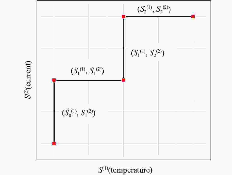
Figure 2. Schematic diagram of the change in stress conditions for the cross-step accelerated degradation test
用
$P\left( t \right)$ 来表示器件在整个试验流程中随应力交叉步进变化的退化曲线。每只器件的退化轨迹曲线都可以表示为分段函数:式中:
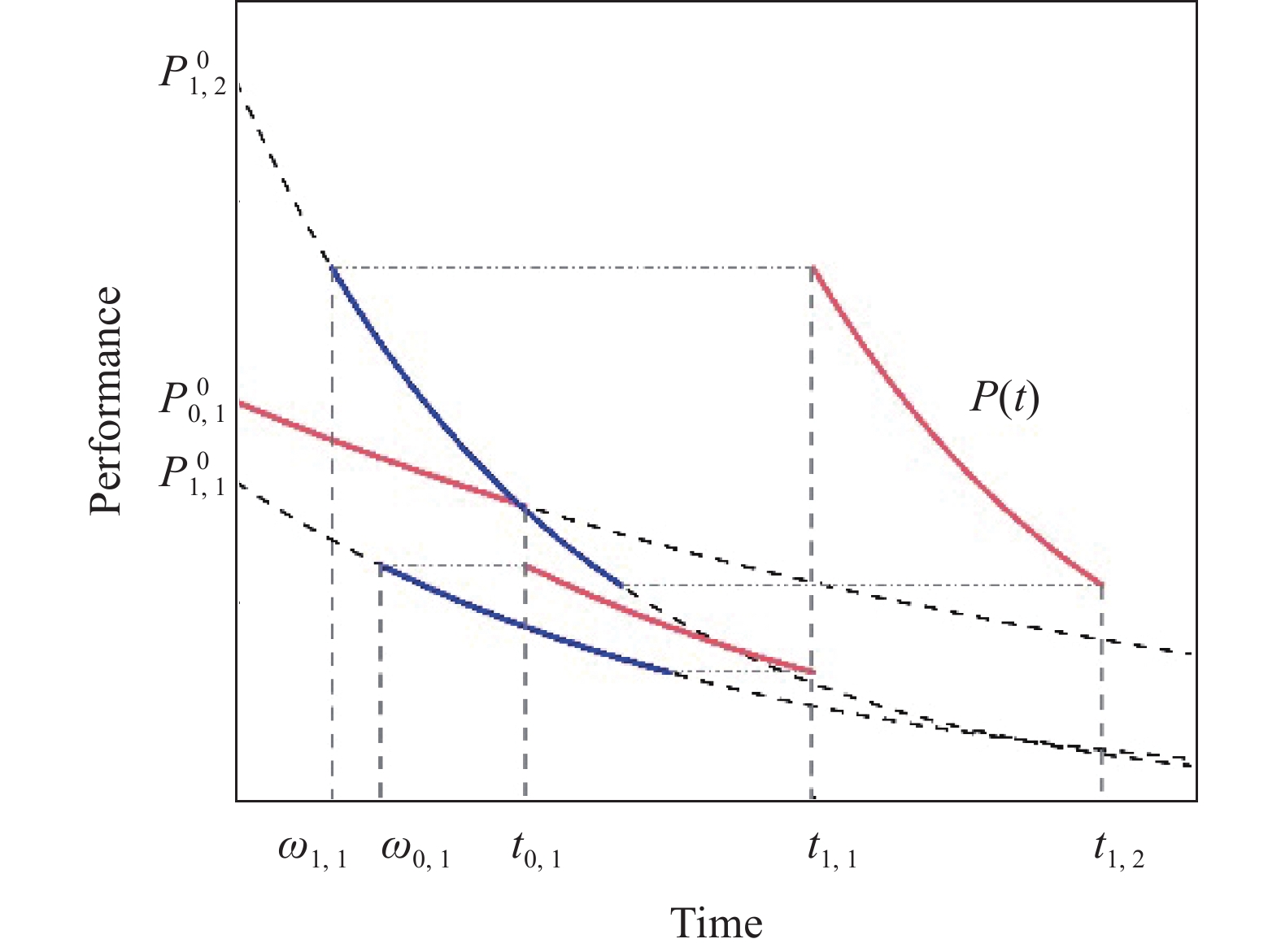
${w_{i,j}}$ 为折算时间,它代表在$ {t}_{i,j} $ 前其他应力水平条件下所有的退化过程折算为下一个应力水平条件下所需的退化时间。从某一加速应力条件折算到另一条件的时间与其退化率之比相关。在应力条件$[S_i^{\left( 1 \right)},S_j^{\left( 2 \right)}]$ 下${w_{i,j}}$ 折算时间可以具体地表示为:这样表示的目的是将某一时刻之前的退化过程全部折算到下一个应力水平条件下,在同一应力水平退化曲线上进行计算[23]。图3表示双应力步进加速退化试验的曲线
$P\left( t \right)$ 与以各个应力条件恒定的加速退化试验曲线$P\left( {t\mid S_i^{\left( 1 \right)},S_j^{\left( 2 \right)}} \right)$ 的换算关系。红色曲线为实际步进应力加速试验得到的性能退化轨迹。它们分别对应着起始就以各自应力条件,进行加速试验得到的性能退化轨迹的蓝色曲线部分。
Figure 3. Conversion relation between
$P\left( t \right)$ and the degradation track$ P\left( {t\mid S_i^{\left( 1 \right)},S_j^{\left( 2 \right)}} \right) $ under each stress condition -
加速模型建立的目的是根据每只器件在各个加速应力条件下的预测寿命外推得到其在额定工作条件下的寿命。
Eyring等人根据量子力学原理进行推导,提出若同时考虑热应力T,电应力I,则关于两个应力可将寿命特征表示为一个函数,据此笔者建立因变量为器件寿命的加速模型,又称广义艾琳模型:
式中:A, B, C, D均为待求参数项;K为玻耳兹曼常数;最后一项为电应力与热应力的交互作用项[24]。
根据加速模型外推得到每只器件的预测寿命,拟合这批器件整体的寿命分布,从而计算MTTF。电子元器件的寿命分布服从威布尔分布[25],计作
$\varepsilon \sim{{W}}\left( {{{m}},{{\eta}}} \right)$ ,它的分布函数和概率密度函数分别为:式中:
${{m}}$ 为形状参数;${{\eta }}$ 为尺度参数。威布尔分布的分布函数可以用来描述一批器件在一段工作时间后的失效百分比。由于实际试验中只能取有限个器件,器件数量为离散变量,那么失效率$ {F}_{i} $ 的无偏估计为:式中:
${n_i}$ 为$ t $ 时间以前(包括$ t $ 时间)所有已经失效的器件数量;$ n $ 为器件总数。 -
文中选取12只830 nm F-mount的单管器件作为研究对象。器件实拍图如图4所示。器件在温度22 ℃下工作,额定工作电流为0.9 A,额定输出功率为1 W。

Figure 4. Photo of experimental 830 nm F-mount single-emitter device
文中自主搭建了大功率半导体激光器单管老化测试平台,如图5所示。平台包括12组器件夹具、Ophir NovaⅡ光功率计、可编程直流电源、可编程步进电机驱动的丝杆滑台、恒温循环冷水机、计算机。该平台集成了控制、监测、试验功能于一体,试验器件功率由PC控制步进电机带动的功率计监测并保存在计算机中[26]。应力设定为温度与电流,并根据单管LIV曲线,温度取22 ℃,42 ℃和62 ℃,电流取1.4 A与1.8 A,两应力条件交叉步进,共组成四种不同的应力条件:A[22 ℃,1.4 A],B[42 ℃,1.4 A],C[42 ℃,1.8 A],D[62 ℃,1.8 A]。在试验中记录全部的光输出功率数据及其对应的应力条件,见表1,器件编号从1#~12#,光输出功率每间隔100 h记录一次,单位W。

Figure 5. Schematic diagram of 830 nm F-mount single-emitter devices accelerated test platform
Stress condition Time/h 1# 2# 3# 4# 5# 6# 7# 8# 9# 10# 11# 12# A[22 ℃,1.4 A] 100 1.43 1.38 1.39 1.41 1.41 1.40 1.36 1.42 1.44 1.36 1.45 1.39 200 1.42 1.38 1.40 1.40 1.40 1.38 1.37 1.43 1.42 1.36 1.44 1.37 300 1.39 1.37 1.37 1.39 1.38 1.35 1.41 1.39 1.39 1.34 1.43 1.34 400 1.40 1.33 1.35 1.40 1.40 1.34 1.34 1.40 1.37 1.35 1.40 1.34 B[42 ℃,1.4 A] 500 1.36 1.33 1.33 1.37 1.38 1.30 1.29 1.36 1.31 1.31 1.36 1.29 600 1.32 1.30 1.29 1.34 1.32 1.27 1.32 1.33 1.28 1.28 1.36 1.31 700 1.28 1.30 1.31 1.34 1.34 1.27 1.29 1.31 1.30 1.27 1.35 1.25 800 1.30 1.29 1.30 1.33 1.30 1.26 1.25 1.30 1.29 1.23 1.31 1.26 C[42 ℃,1.8 A] 900 1.62 1.63 1.62 1.70 1.69 1.64 1.69 1.72 1.70 1.60 1.69 1.69 1000 1.57 1.60 1.59 1.65 1.65 1.60 1.67 1.65 1.68 1.57 1.67 1.69 1100 1.55 1.58 1.50 1.64 1.60 1.57 1.62 1.61 1.61 1.53 1.60 1.63 1200 1.50 1.51 1.52 1.58 1.58 1.50 1.56 1.62 1.57 1.54 1.60 1.56 D[62 ℃,1.8 A] 1300 1.39 1.44 1.43 1.50 1.45 1.39 1.52 1.50 1.47 1.40 1.49 1.42 1400 1.35 1.37 1.38 1.44 1.41 1.33 1.45 1.44 1.40 1.35 1.45 1.41 1500 1.27 1.34 1.33 1.41 1.34 1.31 1.43 1.41 1.35 1.32 1.36 1.35 1600 1.26 1.28 1.27 1.36 1.26 1.25 1.38 1.39 1.29 1.30 1.30 1.30 Table 1. Accelerated degradation test data of 830 nm F-mount single-emitter devices under different stress conditions (optical output power/W)
-
如图6所示,经过1600 h试验后,得到了12只不同器件的实际性能退化数据
$R\left( t \right)$ ,$R\left( t \right)$ 与理论性能退化曲线$P\left( t \right)$ 存在一定误差。为了使理论与实际曲线的程度拟合最大,需要使误差最小化。利用非线性最小二乘拟合,可以得到理论性能退化曲线$P\left( t \right)$ ,即求得实际退化数据$R\left( t \right)$ 与理论退化曲线$P\left( t \right)$ 之差的平方和最小时${\;\beta _{i,j}}$ 的取值。
Figure 6. Performance degradation data of 830 nm F-mount single-emitter devices
由此可以得到
$ \;{\beta }_{i,j} $ 的点估计值,如表2所示。$\; {\beta }_{i,j} $ 随着应力条件的增大而增大,其物理意义是应力条件越高,退化的速度越快。根据公式(1),文中进行双应力交叉步进条件下的加速退化试验共计1600 h,从光输出功率退化量可以反推出[22 ℃ ,1.4 A]条件下需要的退化时间。可以计算得出,四种条件下总计1600 h的加速试验相当于约3783 h在[22 ℃ ,1.4 A]的条件下的恒定应力加速试验。若按照传统的恒定电流加速寿命试验并外推器件的寿命预测方法,则至少需要在试验中设置除[22 ℃,1.4 A]条件以外的两组以上其他条件下的加速试验,相当于节约了大于57.7%的试验时间。Laser
diode IDβ22 ℃,1.4 A β42 ℃,1.4 A β42 ℃,1.8 A β62 ℃,1.8 A 1 $ 9.152\times {10}^{-5} $ $ 1.358\times {10}^{-4} $ $ 2.711\times {10}^{-4} $ $ 3.674\times {10}^{-4} $ 2 $ 9.245\times {10}^{-5} $ $ 1.367\times {10}^{-4} $ $ 2.613\times {10}^{-4} $ $ 3.624\times {10}^{-4} $ 3 $ 8.167\times {10}^{-5} $ $ 1.251\times {10}^{-4} $ $ 2.420\times {10}^{-4} $ $ 3.635\times {10}^{-4} $ 4 $ 8.321\times {10}^{-5} $ $ 1.242\times {10}^{-4} $ $ 2.338\times {10}^{-4} $ $ 3.137\times {10}^{-4} $ 5 $ 8.905\times {10}^{-5} $ $ 1.337\times {10}^{-4} $ $ 2.566\times {10}^{-4} $ $ 3.893\times {10}^{-4} $ 6 $ 9.458\times {10}^{-5} $ $ 1.415\times {10}^{-4} $ $ 2.805\times {10}^{-4} $ $ 3.684\times {10}^{-4} $ 7 $ 7.345\times {10}^{-5} $ $ 1.097\times {10}^{-4} $ $ 2.089\times {10}^{-4} $ $ 3.259\times {10}^{-4} $ 8 $ 7.563\times {10}^{-5} $ $ 1.124\times {10}^{-4} $ $ 2.073\times {10}^{-4} $ $ 3.126\times {10}^{-4} $ 9 $ 9.011\times {10}^{-5} $ $ 1.344\times {10}^{-4} $ $ 2.569\times {10}^{-4} $ $ 3.698\times {10}^{-4} $ 10 $ 8.583\times {10}^{-5} $ $ 1.261\times {10}^{-4} $ $ 2.372\times {10}^{-4} $ $ 3.521\times {10}^{-4} $ 11 $ 9.774\times {10}^{-5} $ $ 1.440\times {10}^{-4} $ $ 2.719\times {10}^{-4} $ $ 3.973\times {10}^{-4} $ 12 $ 9.804\times {10}^{-5} $ $ 1.464\times {10}^{-4} $ $ 2.878\times {10}^{-4} $ $ 3.868\times {10}^{-4} $ Table 2. Degradation rate of each laser diode at each stress condition
为了验证加速模型公式(7)中电流与温度是否存在交互作用,需要检验由样本得到的交互作用项参数
$ d $ 的显著性。只要取两组模型参数(管1和管2共八个退化率数据)进行假设检验,根据统计决策的结果认为存在或不存在交互作用。根据加速退化模型公式(9)作线性方程组进行最小二乘估计得到12组模型参数估计值$ \hat{a},\hat{b},\hat{c},\hat{d} $ ,那么线性方程组可表示为:式中:
$ A $ 为由加速模型组成的系数矩阵;$ b $ 为加速寿命的对数组成的列矩阵,则$x={[\hat{a},\hat{b},\hat{c},\hat{d}]}^{\rm T}$ 的最小二乘估计具体的矩阵计算形式如下:依照上述参数估计方法,得到
$ \hat{a},\hat{b},\hat{c},\hat{d} $ ,如表3所示。$ a $ $ b $ $ c $ $ d $ 4.40 1 830 −1.66 −3.36 Table 3. Parameters of the accelerated degradation model obtained by taking two sets of single-emitter 1 and single-emitter 2 (a total of 8 degradation rate data)
其中广义艾琳模型默认电流、温度应力是交互作用的,即两个变量非独立。需要对交互作用项的存在进行假设检验以确保模型没有多余的变量存在,防止模型出现过拟合。
假设
那么统计量
${{t}}$ 的表达式为:式中:
$ q $ 为自变量个数,在这里取3;$ 2 l $ 代表不同应力水平下的方程个数,取8;$ {s}_{\widehat{d}} $ 为回归系数$ \widehat{d} $ 的抽样分布的标准差。给定显著性水平0.1,查
$t$ 分布表得到$t{\left( {2 l - q - 1} \right)_{0.05}} = 2.131\;8$ 。由$\left| {{t}} \right| = 0.238\;7 < 2.131\;8$ ,所以接受假设${H_0}$ 。因此,模型假设无交互作用项成立。于是加速模型公式(5)改写为:将表2中的
$\; {\beta _{i,j}} $ 代入公式(8)可以求得${\varepsilon _{i,j}}$ 。根据加速退化模型作线性方程组最小二乘估计得到12组模型参数的估计值$\hat a,\hat b,\hat c$ ,如表4所示。Laser diode ID a b c ε22 ℃,0.9 A/h 1 4.01 1 833 −1.73 5805 2 3.90 1 816 −1.62 5420 3 3.51 1 981 −1.65 6249 4 3.80 1 862 −1.58 5942 5 3.73 1 880 −1.63 5630 6 3.81 1 873 −1.71 5542 7 3.95 1 865 −1.61 6789 8 3.89 1 841 −1.53 6334 9 3.79 1 856 −1.62 5561 10 4.02 1 786 −1.58 5722 11 3.85 1 799 −1.59 5001 12 3.81 1 853 −1.69 5273 Table 4. Accelerated degradation model parameters corresponding to each laser diode and extrapolated lifetime
确定加速模型后,将光输出功率下降为初始光功率的80%定为失效标准,将它和标准工作应力条件[22 ℃,0.9 A]代入公式(2)可以得到12只器件的预测寿命
$\varepsilon $ ,如上表所示。由$\varepsilon \sim {{W}}\left( {{{m}},{\textit{η }}} \right)$ ,将威布尔分布函数等式移项后两边同时求对数,利用直线最小二乘估计法求得形状参数${{m}}$ 和尺度参数${\textit{η }}$ 。由公式(6)得到:这样就将威布尔分布函数改写成了关于(
${\rm ln}t$ ,${\rm lnln}{\left[ {1 - F\left( t \right)} \right]^{ - 1}}$ )的一次函数。根据上式进行直线最小二乘法拟合,如图7(a)所示,求得斜率即形状参数m=11.68,再利用截距求得尺度参数η=5994 h。基于威布尔分布的失效分布函数标准形式如图7(b)所示。根据威布尔分布函数的性质,失效率为50%时所对应的时间$t$ 即为MTTF,计算结果为5811 h。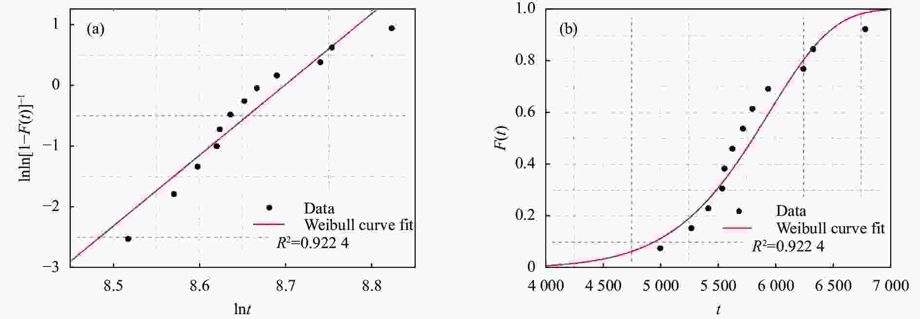
Figure 7. Failure data points were fitted with the curve of Weibull distribution function and the fit was 92.24%. (a) Estimation results of the Weibull plot after coordinate transformation; (b) Fitting results of the failure distribution function
-
如表5所示,不考虑交互作用项,文中使用12个单管器件在A[22 ℃,1.4 A],B[42 ℃,1.4 A],C[42 ℃,1.8 A]三种应力条件下的性能退化数据拟合模型后,计算D[62 ℃,1.8 A]条件下的退化率βtest,并与真实退化率β62 ℃,1.8 A进行对比。误差均在10%以下,说明了文中建立模型的准确性。
Laser diode ID β62 ℃,1.8 A βtest Error 1 $ 3.674\times 1{0}^{-4} $ $ 3.837\times 1{0}^{-4} $ $ 4.44\text{%} $ 2 $ 3.624\times 1{0}^{-4} $ $ 3.686\times 1{0}^{-4} $ $ 1.02\text{%} $ 3 $ 3.635\times 1{0}^{-4} $ $ 3.522\times 1{0}^{-4} $ $ 3.11\text{%} $ 4 $ 3.137\times 1{0}^{-4} $ $ 3.328\times 1{0}^{-4} $ $ 6.09\text{%} $ 5 $ 3.893\times 1{0}^{-4} $ $ 3.657\times 1{0}^{-4} $ $ 6.09\text{%} $ 6 $ 3.684\times 1{0}^{-4} $ $ 4.001\times 1{0}^{-4} $ $ 8.60\text{%} $ 7 $ 3.259\times 1{0}^{-4} $ $ 2.975\times 1{0}^{-4} $ $ 8.71\text{%} $ 8 $ 3.126\times 1{0}^{-4} $ $ 2.939\times 1{0}^{-4} $ $ 5.98\text{%} $ 9 $ 3.698\times 1{0}^{-4} $ $ 3.651\times 1{0}^{-4} $ $ 1.27\text{%} $ 10 $ 3.521\times 1{0}^{-4} $ $ 3.327\times 1{0}^{-4} $ $ 5.51\text{%} $ 11 $ 3.973\times 1{0}^{-4} $ $ 3.824\times 1{0}^{-4} $ $ 3.75\text{%} $ 12 $ 3.868\times 1{0}^{-4} $ $ 4.097\times 1{0}^{-4} $ $ 5.92\text{%} $ Table 5. Comparison of the theoretical degradation rate βtest calculated by the model with the actual degradation rate β62 ℃,1.8 A
-
文中通过自主搭建的试验平台,采用交叉步进四种不同的电流-温度双应力条件对12只830 nm F-mount单管半导体激光器进行了1600 h的加速退化试验,在试验期间记录的光输出功率数据呈缓慢下降的趋势。将退化数据代入排除交互作用项后的艾琳模型中进行参数估计,并结合威布尔分布外推得到器件的MTTF为5811 h。模型也通过了误差低于10%的准确性检验。
文中使用的加速试验方法与传统的单应力恒定加速寿命试验方法相比,节约了大量的试验时间和成本。除此之外,文中使用的双应力交叉步进应力退化试验方法比恒定应力退化试验需要的样本量更少,在实际试验过程中可以根据退化速度调整下一阶段试验的应力条件,具有一定的灵活性。
文中的寿命预测方法研究源于国内大功率半导体激光器与国外的可靠性差距,对于高可靠性半导体激光器的自主研制具有重要的理论和试验价值。
Lifetime prediction method for high-power laser diodes under double-stress cross-step accelerated degradation test
doi: 10.3788/IRLA20220592
- Received Date: 2022-08-17
- Rev Recd Date: 2022-11-16
- Publish Date: 2023-05-25
Fund Project:
National Natural Science Foundation of China (61504167); NaturalScience Foundation of Shaanxi Province, China (2022JQ-531, 2019ZY-CXPT-03-05, 2018JM6010, 2015JQ6263); Shaanxi Provincial Department of Science and Technology Talent Project (2017KJXX-72)
-
Key words:
- high-power laser diodes /
- accelerated degradation test /
- double-stress /
- lifetime
Abstract:


 DownLoad: