


-
脉冲激光探测通过主动发射纳秒级脉冲激光进行目标非接触探测,具有高精度、高分辨率和高效率等优点,已广泛应用于民用、工业和国防等领域[1]。在目标探测时,使用被测物体的距离和回波的强度信息进行探测识别[2]。脉冲回波信号的强度获取方法主要有峰值检测法[3]、脉宽测量法[4]和全波形采样法等[5]。其中脉宽测量法易受探测目标外形影响从而改变回波脉宽;全波形采样法实时采样整个时域回波[6],对于窄脉冲信号需要高速模数转换器(Analog to Digi-tal Converter,ADC),对器件要求高[7],且成本和功耗难以降低。峰值检测法通过跟踪保持回波脉冲峰值,展宽脉冲信号宽度,可有效降低对ADC的性能要求。
峰值检测电路作为脉冲激光探测系统中的重要功能模块,国内外科研机构对其已开展了较多的相关研究。印度班加罗尔理工学院的P. Lipika等人采用0.18 μm CMOS工艺设计了具有62.19 dB增益和单位增益带宽为14 MHz的峰值采样保持电路[8]。西安电子科技大学郑浩等人采用复位至共模电压和充电电流自动调节的方法来减小峰值输出误差,电路可探测的最小脉冲宽度为5 ns,输出误差小于4.5%[9]。中国科学院空天信息创新研究院王峰奇等人采用SMIC 0.18 μm的工艺仿真设计了一款动态范围为800 mV,脉宽3 ns的峰值保持电路,仿真结果表明该电路的脉冲保持电压误差小于3.16%[10]。
当前研究工作主要针对单一回波进行峰值探测,对多回波峰值探测相关研究相对较少。针对脉冲激光探测系统在复杂场景下多回波检测的应用需求,文中对脉冲多回波产生机理和峰值检测电路进行研究,采用交织采样和多路复用技术,设计完成了一种适用于脉冲激光多回波探测的新型两级峰值检测电路芯片。同时,研究峰值检测电路输出误差与通道数的关系,并搭建测试平台对所设计的电路芯片进行测试验证。
-
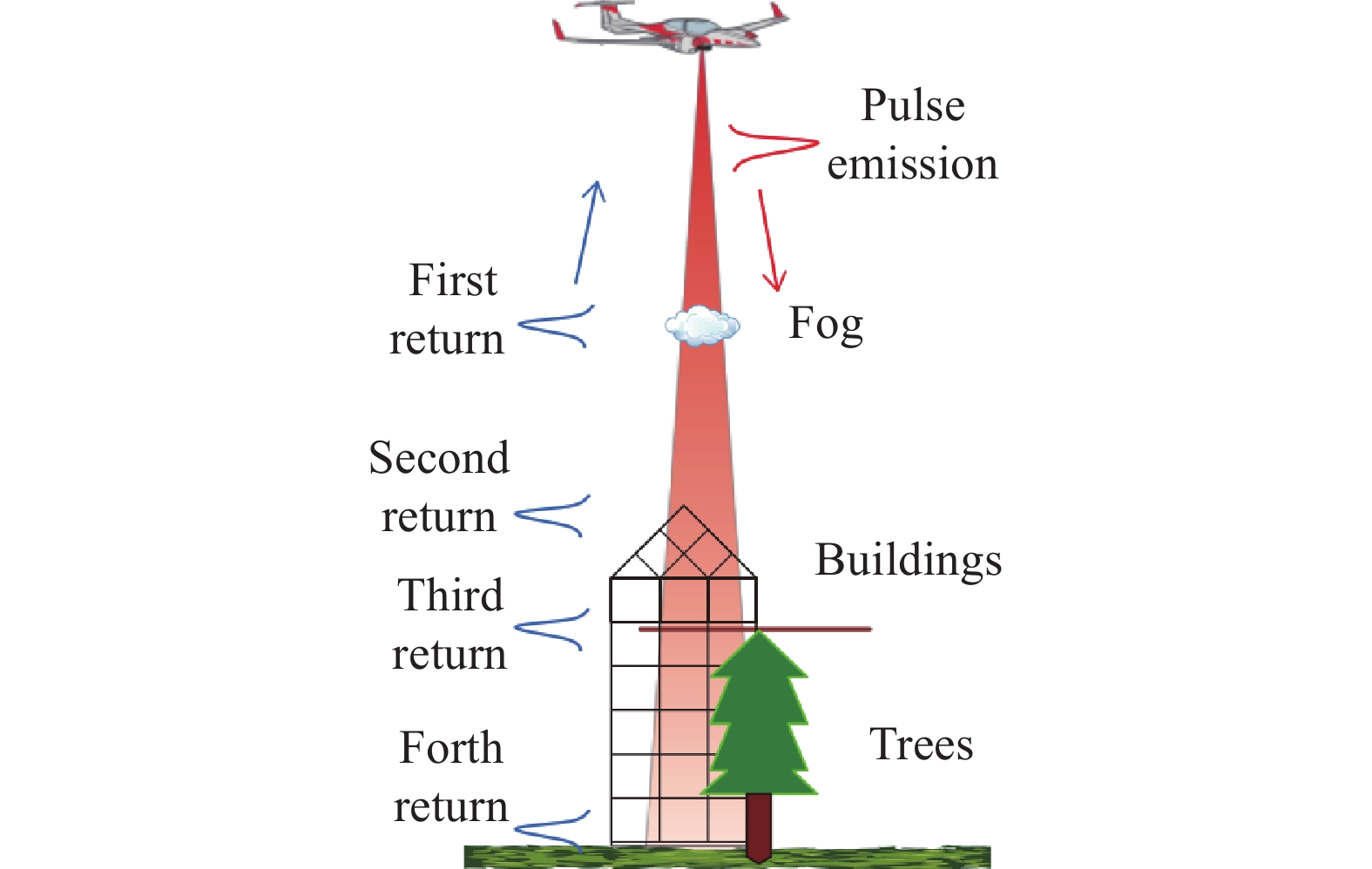
由于脉冲激光探测的固有特性[11],如图1所示,激光具有一定的发散角,当激光照射到部分反射或部分遮挡的雾、粉尘、建筑物和树冠[12]等空间分布多层物体时会产生多次反射回波[13]。

Figure 1. Typical multi-echo phenomenon
根据目标大小与激光光斑面积的关系,常把目标分为点、线、面三种。以点目标为例,设激光发散角为θ,激光雷达距离方程为[14]:
式中:Pr为回波功率;Pt为发射脉冲功率;ρ为目标反射率;η为收发光学系统效率;Ta为激光大气单程透过率;Ar为接收光学口径;α为光束与目标法线的夹角;R为探测距离;At为光斑照在目标上的截面积。根据公式(1),在复杂场景下,当这些回波能量高于系统探测阈值时,就会被系统探测到,并且在目标反射率接近的情况下,近处物体的回波峰值能量一般相对较大,易对较远处的回波造成“遮挡”,因此通过多回波峰值检测,可以使探测系统具备更精细的多层次探测能力和更强的抗干扰能力。
-
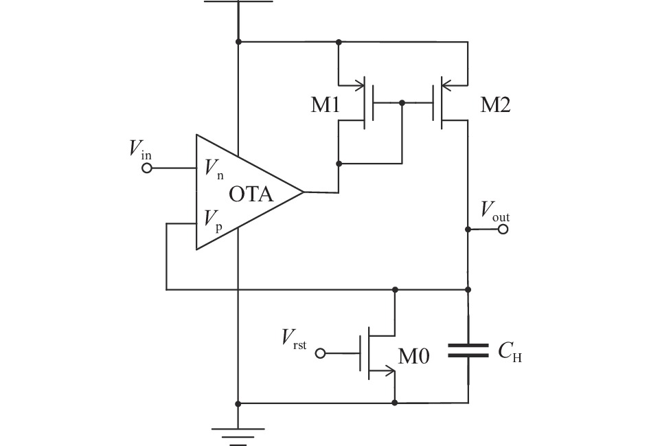
典型的峰值检测采样保持(Peak Detector Sample and Hold,PDSH)电路[15]如图2所示,由跨导放大器(Operational Transconductance Amplifier,OTA)、电流镜、采样保持电容CH和复位开关M0等器件组成。OTA电路采用差分放大器,通过电流镜结构实现单向导通功能对电容充电。当电路的输入端Vin检测到正向脉冲信号时,OTA的输出电压迅速变低,M2导通给电容CH充电,使输出电压Vout等于输入脉冲电压的峰值。当输入脉冲电压下降时,M2关断,电容CH上的电荷保持不变,直至复位信号Vrst开启M0进行放电复位。

Figure 2. Schematic of PDSH circuit
峰值检测采样保持电路误差模型如图3所示,电路的输出电压误差VE主要受OTA和M2器件参数的影响,包括峰值电压误差(Peak Error, PKE)和基底电压误差(Pedestal Error, PDE),其中峰值电压VPKE主要为过冲电压,基底电压误差VPDE表示为[16]:
式中:VG,M2为M2的栅压;VO,CM、A、VOS、CMRR分别为OTA的输出共模电压、开环增益、偏移电压、共模抑制比;Vin、VCM分别为输入信号电压和共模电压。在多回波峰值检测电路中,多个回波通道间的OTA增益、共模抑制比和偏移电压等差异会增大电路的输出误差,因此需要优化设计以减少上述偏差。

Figure 3. Error model of PDSH circuit
-
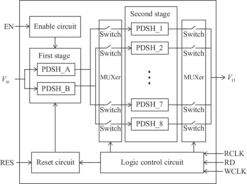
文中设计的前端放大器线性输出范围为500 mV,脉冲回波信号为脉宽5 ns,因此,脉冲峰值检测电路需要有较快的响应速度才能检测到窄脉冲峰值,带来的挑战是在电路中设计的保持电容容值受限,导致保持输出时间短;另一方面,为了保持精度和保持时间又需要采用容值大的保持电容。为了缓解上述问题,满足窄脉冲峰值检测和长时间峰值保持的要求,文中设计采用两级峰值检测保持电路的结构,通过第一级电路对窄脉冲峰值信号进行快速采样,展宽脉冲,再用第二级电路实现信号的长时间保持。同时,所应用的激光探测系统设计要能检测八个回波脉冲峰值,为了实现多回波探测,传统方法一般需要有多个峰值检测电路并联工作,整体电路结构复杂,功耗和面积大,因此,设计中采用了交织采样和多路复用的方法对两级峰值检测电路结构进行了精简优化。
所设计的多回波脉冲峰值检测电路整体框架如图4所示,由复用的第一级双通道PDSH电路和第二级八路PDSH电路、级间输入、输出多路选择电路、开启电路、复位电路和逻辑控制电路组成。首先检测电路开启第一级PDSH_A和第二级PDSH_1电路,对第一个脉冲回波信号进行峰值采样保持;当第二个脉冲回波到来时,输入切换至电路中的PDSH_B和PDSH_2电路,实现对第二回波峰值检测采样保持,同时复位PDSH_A电路;当第三个回波到来时,输入切换至电路中的PDSH_A和PDSH_3电路并复位PDSH_B电路,后续采用同样的方法,通过复用第一级PDSH电路对多回波进行交替采样,实现对多回波脉冲的快速采样和脉宽展宽;第二级PDSH电路依次接收前级展宽的信号并进行长时间保持。Vin为回波输入接口,VO为输出接口,EN电路开启/关闭接口,RES为复位接口,RCLK为输出控制接口,控制信号输出时间,RD为读写控制接口,WCLK为级间控制接口,与回波信号相关联。

Figure 4. Schematic of multi-echo peak detection circuit
通过对第一级双通道PDSH电路的复用,不仅降低了面积和功耗,同时也降低了电路的输出误差。根据图3的峰值检测采样保持电路的误差模型,得到输出误差Verr为:
式中:VOS为输入偏移;Ve,Ci+Cc为输入管的寄生电容造成的误差;MOS管M2的寄生电容造成的误差Ve,Cd+Cgd远小于Ve,Ci+Cc,因此可以忽略。输入偏移VOS和Ve,Ci+Cc分别为:
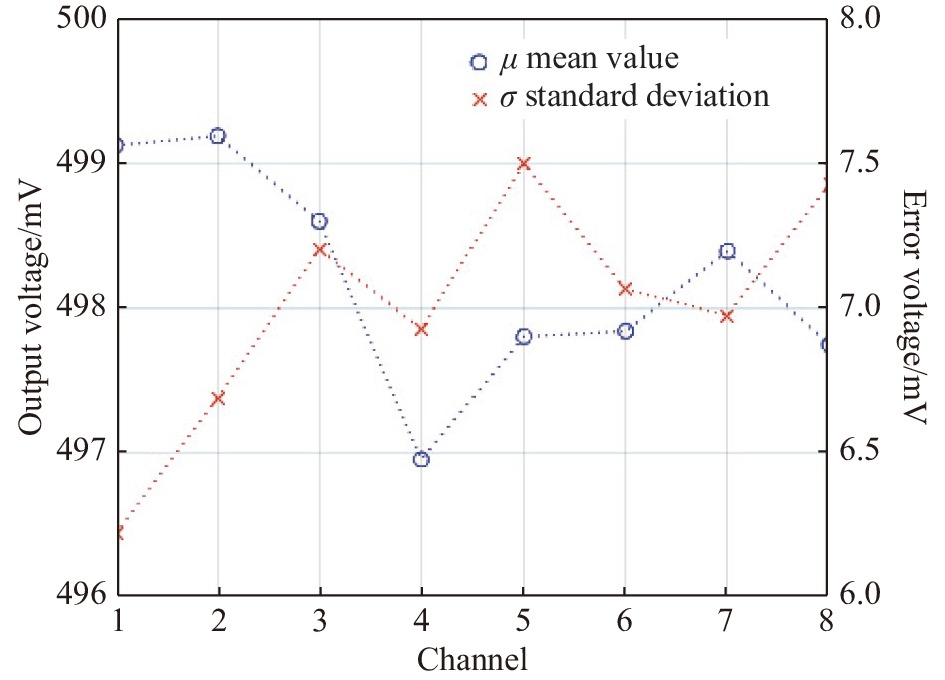
式中:Wi、Li、ΔW和ΔL分别为输入管的宽与长以及相应的偏差;β、κ为与工艺相关的系数。通过对第一级采用不同通道数的峰值检测电路进行蒙特卡洛仿真,当输入脉冲幅值为500 mV,脉宽为5 ns时,电路的电压输出平均值和标准差结果如图 5所示,通道数的增多会在一定程度上增大电路输出误差。因此,在第一级通过复用峰值采样电路减少了所需的通道数,可有效提高峰值检测电路的输出精度。

Figure 5. Simulaion output with different channel numbers (input pulse amplitude of 500 mV, pulse width of 5 ns)
-
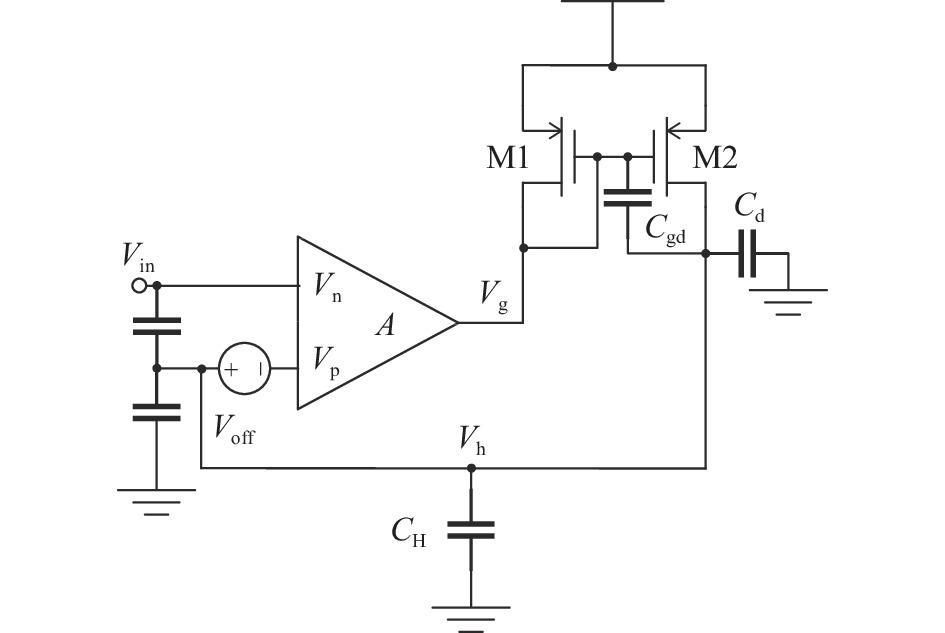
第一级电路中的两个子模块PDSH_A和PDSH_B内部结构相同,如图6所示,采用单端输出的两级运放结构,通过电流镜为电容充电来实现峰值采集功能。当放大器的两个输入端存在电压差时,输出端处将会产生电流,由MP4、MP5构成的电流镜为电容充电,电容上的电压经MP7的源端反馈到差动运放的正输入端,构成一个反馈电路跟踪输入信号。MP5管与电容CH构成充电支路,无法对其进行放电,所以在输入信号达到峰值后开始衰减时,电容上的电压值保留了其最大值,进而实现了输入信号峰值保持的作用。复位电路由MN0构成,当接收到复位信号Vres后,MOS管导通,快速泄放掉电容CH上的电荷进行复位。

Figure 6. First stage PDSH circuit
放大器的直流增益A0为:
式中:gm,MN1为MN1的跨导;rO,MN2与rO,MP2分别为MN2与MP2的等效阻抗;gm,MP3与gm,MP4分别为MP3和MP4的跨导;rO,MN4与rO,MP3分别为MN4与MP3的等效阻抗。
对于窄脉冲信号,保持电容的选取需要满足快速充电的要求,才能准确快速检测到峰值电压。容值大小可依据压摆率SR公式进行选取:
式中:I为充电电流;CH为保持电容;ΔUi,Δt分别为变化的电压和时间。在压摆率一定的情况下,尽量选择小电容以减小电流降低电路功耗。对于500 mV信号,5 ns脉宽上升时间取2 ns,压摆率为250 V/μs,根据公式(7),I取100 μA,得到第一级PDSH电路的保持电容取值需要小于0.4 pF。
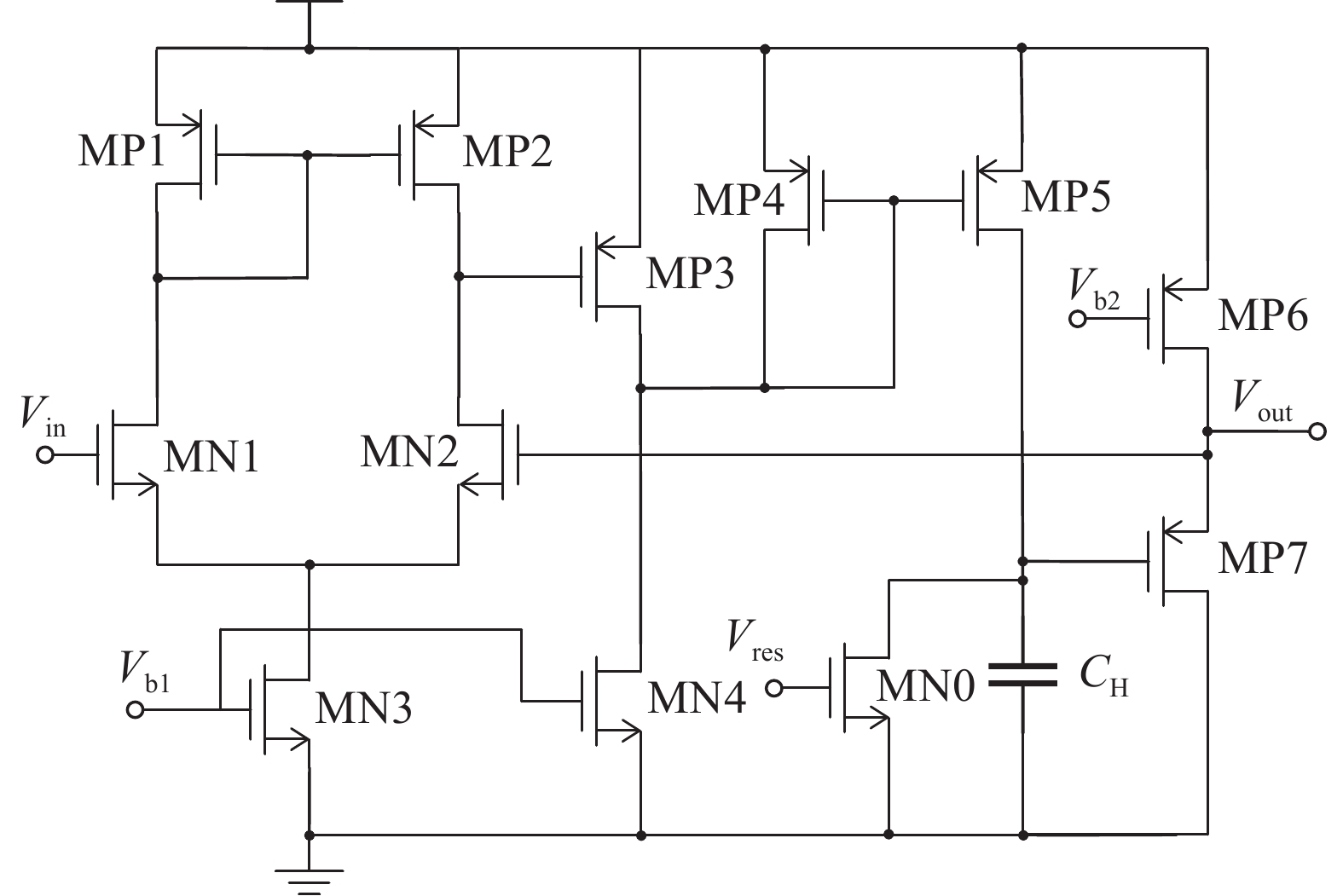
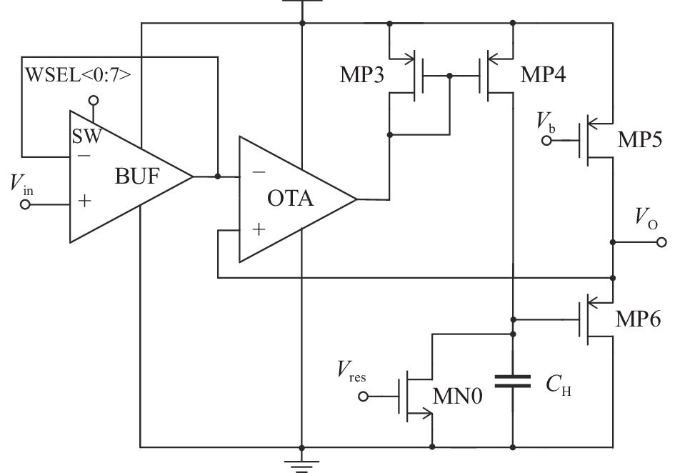
第二级电路中的PDSH_1~8电路结构如图7所示,OTA内部结构与上述第一级中的OTA电路相同,前端驱动BUF电路作为通道控制电路,通过级间控制信号在开关电路的控制下实现对前端电路的输出采样保持。通过采用两级峰值检测电路,第一级电路进行快速准确的峰值采样,第二级电路实现较长时间脉冲峰值电压的保持,有效解决了窄脉冲精确检测与长时间保持的问题,提高了信号检测的精度。

Figure 7. Second stage of PDSH circuit
-
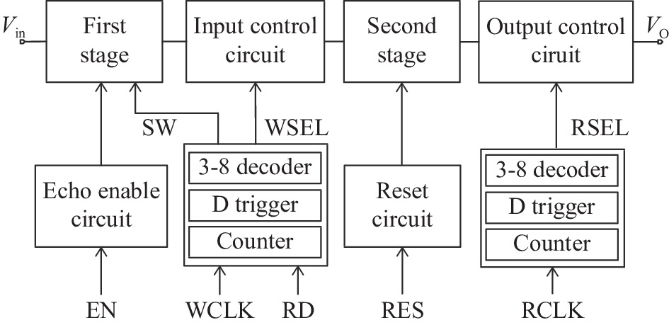
逻辑控制电路如图8所示,包含开启电路、复位电路、级间输入控制电路和输出控制电路四个部分。开启电路由反相器组构成,当EN信号电平为低时开启电路工作。复位电路由RES信号控制,由开关管构成,实现全局复位。第一级复位电路、级间输入和输出控制电路分别受信号SW、WSEL和RSEL控制,由外部信号WCLK、RD和RCLK通过内部所设计的计数器、D触发器、38译码器和编码器等电路产生,实现第一级PDSH电路的复位和通道选通功能。

Figure 8. Block diagram of control circuit
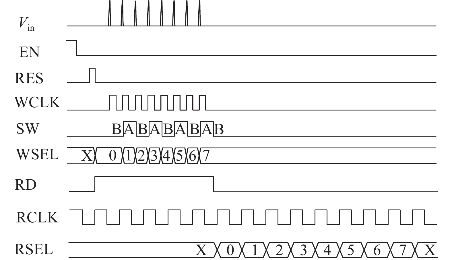
逻辑控制电路的时序如图9所示,电路接收到EN开启和RES复位信号后,芯片开启并全局复位,两级PDSH电路开始工作,对输入信号Vin进行峰值采样保持。WCLK信号输入至内部产生开关选通信号WSEL进行级间通道切换,同时产生SW复位信号在低电平时复位PDSH_B,高电平时复位PDSH_A,交替对第一级的两个PDSH电路复位。RD为读写信号,高电平时电路进行多回波峰值采集,低电平时电路按照输出信号RSEL依次输出。

Figure 9. Time sequence of the logic control
-
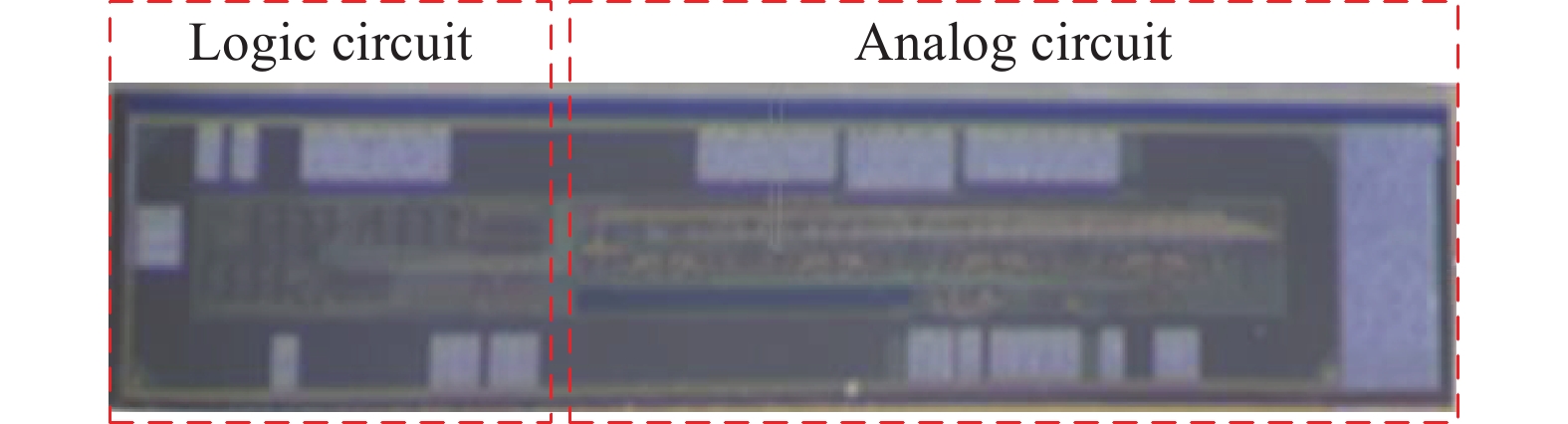
多回波峰值检测电路芯片采用CMOS 0.18 μm工艺设计和流片,芯片显微照片如图10所示,面积尺寸为2.6 mm×0.48 mm。在多回波峰值检测电路版图设计中,除了基本的对称式布局以克服器件的失配等设计原则外,根据电路的仿真结果,需避免数字信号控制开关电路翻转时产生的噪声,干扰两级峰值检测采样电路。在设计时,把数字逻辑电路和模拟电路严格分开布局,并且通过添加多层保护环的方法增强隔离,防止串扰。对于噪声敏感的第一级峰值检测采样保持电路需要单独放置,与其他后端电路隔离,减小外围电路的噪声干扰。同时,由于采用了复用前级的方法减少了相关模拟电路的数量,使得布线相对简单,信号线的走线距离可以更宽,减少了信号线间的耦合影响。

Figure 10. Micrograph of multi-echo peak detection circuit
-
测试过程中,在测试场景内布置八 个靶标,通过调整激光器光斑和靶标的相对位置,使每个靶标的侧边缘都能够被光斑照射,产生八个脉冲回波。测试板外接1.8 V和3.3 V电源,控制板卡接5 V电源。逻辑控制板通过串口控制1550 nm的光纤脉冲激光器,产生脉宽5 ns,频率100 kHz的脉冲信号,同时,通过逻辑控制板产生开启信号、读写时钟以及复位信号。
多回波峰值检测电路芯片测试输出结果如图11所示,芯片在接收到EN开启信号和RES复位信号后开始工作,读写控制通过信号RD进行控制,每个通道输出时间由周期为1 μs的RCLK时钟信号控制,经过八个时钟周期后电路输出信号完成,自动复位。测试的激光发射频率为100 kHz,回波脉宽为5 ns,幅值为50 mV。每个通道均能够正常输出,芯片工作正常。

Figure 11. Measured transient response
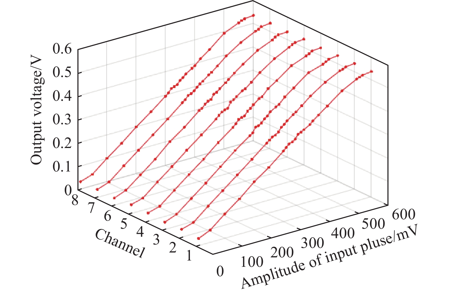
多回波峰值检测电路芯片在信号脉宽为5 ns时,通过调节激光器输出功率,测得芯片在不同回波幅值下的输出电压结果如图12所示,输出电压随着输入回波信号幅值的增大而增大。在输入信号峰值电压为50~500 mV的范围内,芯片的输出电压具有较好的线性度,电路的峰值输出电压的最大误差为4.8%,当输入峰值电压为300 mV时,输出电压相对偏差为1.67%。

Figure 12. Measured results of input and output amplitudes of each channel
在回波脉宽5 ns,幅度50~500 mV的范围内,通过计算相同输入电平时,不同通道间最大最小值之差与平均值的百分比,得到通道间输出电压相对偏差的测试结果如图13所示,通道间的输出电压最大相对偏差为5.7%,当输入峰值电压为300 mV时,通道间的输出电压相对偏差为2.33%。

Figure 13. Measured results of relative error of output voltage between channels
表1给出了多回波峰值检测电路芯片的主要参数与最近相关文献中的电路性能对比。与文献[9]的测试结果和文献[10]的仿真结果相比,所设计的电路芯片能够对脉冲多回波信号进行有效峰值检测,具有较高的检测输出精度,且功耗相近。
-
基于多回波脉冲的时空特性,文中通过采用交织采样技术和多路复用方法设计了一种新型多脉冲回波峰值检测电路芯片,并进行了流片与集成测试。相较于普通多脉冲峰值检测电路,文中的两级电路方案具有更精简的电路结构、更低的通道间峰值检测误差。芯片采用CMOS 0.18 μm工艺设计,测试结果表明,该芯片电路对于5 ns脉宽的多回波脉冲,在50~500 mV的幅值范围内的输出具有良好的线性度,相较于其他窄脉冲峰值检测电路适用性更强,检测能力更优。
Design of pulse laser multi-echo peak detection circuit
doi: 10.3788/IRLA20220625
- Received Date: 2022-08-31
- Rev Recd Date: 2022-12-30
- Publish Date: 2023-05-25
-
Key words:
- laser detection /
- peak-holding circuit /
- multi-echo /
- peak detection
Abstract:


 DownLoad: