Volume 52 Issue 12
Dec.  2023
Turn off MathJax
Article Contents

Yin Zhijun, Wang Zhenxing, Li Quan, Song Renkang, Deng Xiao, Lei Lihua. Research on precise measurement of phonon-polariton interference fringe period[J]. Infrared and Laser Engineering, 2023, 52(12): 20230414. doi: 10.3788/IRLA20230414
Citation: Yin Zhijun, Wang Zhenxing, Li Quan, Song Renkang, Deng Xiao, Lei Lihua. Research on precise measurement of phonon-polariton interference fringe period[J]. Infrared and Laser Engineering, 2023, 52(12): 20230414. doi: 10.3788/IRLA20230414

Research on precise measurement of phonon-polariton interference fringe period

doi: 10.3788/IRLA20230414
Funds:  National Natural Science Foundation of China (62075165, 62175188); National Key Research and Development Program of China (2022YFF0605502); Special Development Funds for Major Projects of Shanghai Zhangjiang National Independent Innovation Demonstration Zone (ZJ2021-ZD-008); Natural Science Foundation of Shanghai (23ZR1465800)
  • Received Date: 2023-07-20
  • Rev Recd Date: 2023-08-15
  • Available Online: 2023-12-22
  • Publish Date: 2023-12-22
  •   Objective  Two-dimensional materials have garnered widespread attention due to their unique photoelectric properties at the nanoscale, showcasing distinctive application advantages in the fields of nano-electronic devices, optics, and energy. Notably, the phonon polaritons generated by the coupled excitation of phonons and photons in two-dimensional materials exhibit highly localized at the nanometer scale, presenting substantial application potential in cutting-edge research fields such as optical manipulation and energy transmission of on-chip photonics. Infrared imaging of the sample revealed that at the sample's edge, the mutual interference of phonon polaritons resulted in the fomation of polarization standing wave fringes parallel to the edge. The fringe period effectively reflects the coupling characteristics of phonon polaritons. Therefore, the study of modulated phonon polariton coupling primarily relies on the precise measurement of the interference fringe period. The current measurement method depends on the linear fitting calculation of image analysis software, and its accuracy is constrained by the image resolution. Additionally, the displacement errors occur in the sample loading stage of SNOM. To enhance measurement accuracy and minimize the impact of the these errors on the measured value, this paper proposes the use a self-traceable chromium grating for the precise measurement of the period of the polariton interference fringe in hBN.   Methods  In this paper, we present a self-traceable grating-hBN composite structure. The construction involves depositing a chromium grating on the silicon substrate using atomic lithography. The gaps between adjacent grating structures consist of air, and the two-dimensional polar material hBN is placed on the chromium grating. The dispersion of phonon polaritons generated by the recombination of hBN and different media is analyzed using Fabry-Perot quantization conditions. The study further investigates the phonon polariton coupling enhancement and modulation characteristics of two-dimensional polar materials resulting from periodic changes in metal grating structures. Scanning near-field optical microscopy (SNOM) was employed to image the phonon polaritons of the composite structure in near-field space during sample processing. Imaging of different sizes is conducted at the same point, and two methods are employed for image processing for comparison. The first method involves traditional linear fitting based on Gwyddion for calculating the interference fringe period, while the second one utilizes the use of image analysis program to perform self-traceable grating comparison measurement on the fringe period.   Results and Discussions  When using the traditional Gwyddion-based linear fitting for calculating the interference fringe period, the measured fringe period in the 1 µm×1 µm near-field optical imaging is 0.264 µm, in the 5 µm×5 µm image is 0.254 µm, and in the 10 µm×10 µm image is 0.257 µm. It is observed that when the size of the measurement image is small, the error offset is large. After a large-scale scanning, the measurement value tends to stabilize, yet the overall measurement result remains unstable. Considering the 10 nm resolution of SNOM, the standard deviation value is calculated as 4 nm. Simultaneously, the image analysis program is employed to perform self-traceable grating comparison measurement on the fringe period, The grating period serves as the scale for measuring the interference fringe period. The fringe periods measured in 1 µm×1 µm, 5 µm×5 µm and 10 µm×10 µm images are 261.28 nm, 260.35 nm, 261.41 nm respectively, with a standard deviation of the measured values at 0.34 nm. Compared with the standard deviation of 4 nm from the traditional measurement method, this presents an order of magnitude reduction, achieving higher precision. When the self-traceable grating is employed, it not only measure the period size, but also calibrate the measurement point of the detection equipment. Taking SNOM in this study as an example, the calibration size ΔU of the equipment displacement device is approximately −0.18 nm/pt, with uncertainty related to the grating uncertainty, achieving sub-nanometer accuracy. However, the actual measurement still needs to consider the impact of the device resolution on measurement accuracy.   Conclusions  By constructing a composite structure comprising a self-traceable chromium grating and a two-dimensional polar material hBN, this study leverages the periodic enhancement principle of phonon polariton intensity generated by the structural changes in the substrate grating material. Employing a scanning near-field optical microscope for imaging, the resulting composite structure exhibits coupling-enhancing fringes consistent with the self-tracing grating pitch distribution. Through image analysis and measurement, the self-traceable grating period of 212.782 nm is utilized as the scale. The interference fringe period is measured to be (261.01±0.34) nm, achieving a measurement with higher accuracy than the uncertainty of the traditional fitting method. Simultaneously, nanoscale calibration of the device can be realized based on the measurement results. In this paper, the imaging calibration of the SNOM device is determined to be −0.18 nm/pt, with uncertainty linked to the grating uncertainty. This grating metrology method offers a measurement approach with superior accuracy and reliability for precisely measuring the excitation wavelength of phonon polaritons and controlling the coupling of photon and phonon. Additionally, it provides an experimental basis for the design and regulation of two-dimensional materials applied to nanoscale devices.
  • [1] Montblanch A, Barbone M, Aharonovich I, et al. Layered materials as a platform for quantum technologies [J]. Nat Nanotechnol, 2023, 18(6): 555-571. doi:  10.1038/s41565-023-01354-x
    [2] Rohaizad N, Mayorga-martinez C, Fojtů M, et al. Two-dimensional materials in biomedical, biosensing and sensing applications [J]. Chem Soc Rev, 2021, 50(1): 619-657. doi:  10.1039/D0CS00150C
    [3] Shanmugam V, Mensah R, Babu K, et al. A review of the synthesis, properties, and applications of 2D materials [J]. Particle & Particle Systems Characterization, 2022, 39(6): 2200031. doi:  10.1002/ppsc.202200031
    [4] Lemme M, Akinwande D, Huyghebaert C, et al. 2D materials for future heterogeneous electronics [J]. Nat Commun, 2022, 13(1): 1392. doi:  10.1038/s41467-022-29001-4
    [5] Novoselov K, Fal′ko V I, Colombo L, et al. A roadmap for graphene [J]. Nature, 2012, 490(7419): 192-200. doi:  10.1038/nature11458
    [6] Caldwell J D, Aharonovich I, Cassabois G, et al. Photonics with hexagonal boron nitride [J]. Nat Rev Mater, 2019, 4(8): 552-567. doi:  10.1038/s41578-019-0124-1
    [7] Tran T, Bray K, Ford M J, et al. Quantum emission from hexagonal boron nitride monolayers [J]. Materials Science, 2016, 11: 37-41. doi:  https://doi.org/10.1038/nnano.2015.242
    [8] Cuadra J, Baranov D G, Wersäll M, et al. Observation of tunable charged exciton polaritons in hybrid monolayer WS2-plasmonic nanoantenna system [J]. Nano Lett, 2018, 18(3): 1777-1785. doi:  10.1021/acs.nanolett.7b04965
    [9] Mitioglu A, Plochocka P, Jadczak J N, et al. Optical manipulation of the exciton charge state in single layer tungsten disulfide [J]. Phys Rev B, 2013, 88(24): 245403. doi:  10.1103/PhysRevB.88.245403
    [10] Jin C, Regan E, Yan A, et al. Observation of moiré excitons in WSe2/WS2 heterostructure superlattices [J]. Nature, 2019, 567(7746): 76-80. doi:  10.1038/s41586-019-0976-y
    [11] Shen S, Narayanaswamy A, Chen G. Surface phonon polaritons mediated energy transfer between nanoscale gaps [J]. Nano Lett, 2009, 9(8): 2909-2913. doi:  10.1021/nl901208v
    [12] Folland T, Fali A, White S, et al. Reconfigurable mid-infrared hyperbolic metasurfaces using phase-change materials [J]. Nat Commun, 2018, 9(1): 4371. doi:  10.1038/s41467-018-06858-y
    [13] Chaudhary K, Tamagnone M, Yin X, et al. Polariton nanophotonics using phase-change materials [J]. Nat Commun, 2019, 10(1): 4487. doi:  10.1038/s41467-019-12439-4
    [14] Dai S, Ma Q, Liu M K, et al. Graphene on hexagonal boron nitride as a tunable hyperbolic metamaterial [J]. Nature Nanotech, 2015, 10(8): 682-686. doi:  10.1038/nnano.2015.131
    [15] Li P, Hu G, Dolado I, et al. Collective near-field coupling and nonlocal phenomena in infrared-phononic metasurfaces for nano-light canalization [J]. Nature Communications, 2020, 11: 3663. doi:  10.1038/s41467-020-17425-9
    [16] Li P, Dolado I, Alfaro-mozaz F J, et al. Infrared hyperbolic metasurface based on nanostructured van der waals materials [J]. Science, 2018, 359(6378): 892-896. doi:  10.1126/science.aaq1704
    [17] Dai S, Ma Q, Andersen T, et al. Subdiffractional focusing and guiding of polaritonic rays in a natural hyperbolic material [J]. Nat Commun, 2015, 6(1): 6963. doi:  10.1038/ncomms7963
    [18] Balykin V I, Letokhov V S. The possibility of deep laser focusing of an atomic beam into the Å-region [J]. Optics Communications, 1987, 64(2): 151-156. doi:  10.1016/0030-4018(87)90042-3
    [19] Mcclelland J. Atom-optical properties of a standing-wave light field [J]. J Opt Soc Am B, 1995, 12(10): 1761. doi:  10.1364/JOSAB.12.001761
    [20] Mcclelland J, Anderson W R, Bradley C, et al. Accuracy of nanoscale pitch standards fabricated by laser-focused atomic deposition [J]. J Res Natl Inst Stand Technol, 2003, 108(2): 99. doi:  10.6028/jres.108.0010
    [21] Deng X, Lin Z, Dai G, et al. Length traceability chain based on chromium atom transition frequency[EB/OL]. (2023-02-23)[2023-07-20]. https://arxiv.org/abs/2302.14633.
  • 加载中
通讯作者: 陈斌, bchen63@163.com
  • 1. 

    沈阳化工大学材料科学与工程学院 沈阳 110142

  1. 本站搜索
  2. 百度学术搜索
  3. 万方数据库搜索
  4. CNKI搜索

Figures(5)  / Tables(1)

Article Metrics

Article views(128) PDF downloads(48) Cited by()

Related
Proportional views

Research on precise measurement of phonon-polariton interference fringe period

doi: 10.3788/IRLA20230414
  • 1. School of Physics Science and Engineering, Tongji University, Shanghai 200092, China
  • 2. Institute of Precision Optical Engineering, Tongji University, Shanghai 200092, China
  • 3. MOE Key Laboratory of Advanced Micro-Structured Materials, Shanghai 200092, China
  • 4. Shanghai Frontiers Science Center of Digital Optics, Shanghai 200092, China
  • 5. Shanghai Professional Technical Service Platform for Full-Spectrum and High-Performance Optical Thin Film Devices and Applications, Shanghai 200092, China
  • 6. Shanghai Institute of Measurement and Testing Technology, Shanghai 201203, China
Fund Project:  National Natural Science Foundation of China (62075165, 62175188); National Key Research and Development Program of China (2022YFF0605502); Special Development Funds for Major Projects of Shanghai Zhangjiang National Independent Innovation Demonstration Zone (ZJ2021-ZD-008); Natural Science Foundation of Shanghai (23ZR1465800)

Abstract:   Objective  Two-dimensional materials have garnered widespread attention due to their unique photoelectric properties at the nanoscale, showcasing distinctive application advantages in the fields of nano-electronic devices, optics, and energy. Notably, the phonon polaritons generated by the coupled excitation of phonons and photons in two-dimensional materials exhibit highly localized at the nanometer scale, presenting substantial application potential in cutting-edge research fields such as optical manipulation and energy transmission of on-chip photonics. Infrared imaging of the sample revealed that at the sample's edge, the mutual interference of phonon polaritons resulted in the fomation of polarization standing wave fringes parallel to the edge. The fringe period effectively reflects the coupling characteristics of phonon polaritons. Therefore, the study of modulated phonon polariton coupling primarily relies on the precise measurement of the interference fringe period. The current measurement method depends on the linear fitting calculation of image analysis software, and its accuracy is constrained by the image resolution. Additionally, the displacement errors occur in the sample loading stage of SNOM. To enhance measurement accuracy and minimize the impact of the these errors on the measured value, this paper proposes the use a self-traceable chromium grating for the precise measurement of the period of the polariton interference fringe in hBN.   Methods  In this paper, we present a self-traceable grating-hBN composite structure. The construction involves depositing a chromium grating on the silicon substrate using atomic lithography. The gaps between adjacent grating structures consist of air, and the two-dimensional polar material hBN is placed on the chromium grating. The dispersion of phonon polaritons generated by the recombination of hBN and different media is analyzed using Fabry-Perot quantization conditions. The study further investigates the phonon polariton coupling enhancement and modulation characteristics of two-dimensional polar materials resulting from periodic changes in metal grating structures. Scanning near-field optical microscopy (SNOM) was employed to image the phonon polaritons of the composite structure in near-field space during sample processing. Imaging of different sizes is conducted at the same point, and two methods are employed for image processing for comparison. The first method involves traditional linear fitting based on Gwyddion for calculating the interference fringe period, while the second one utilizes the use of image analysis program to perform self-traceable grating comparison measurement on the fringe period.   Results and Discussions  When using the traditional Gwyddion-based linear fitting for calculating the interference fringe period, the measured fringe period in the 1 µm×1 µm near-field optical imaging is 0.264 µm, in the 5 µm×5 µm image is 0.254 µm, and in the 10 µm×10 µm image is 0.257 µm. It is observed that when the size of the measurement image is small, the error offset is large. After a large-scale scanning, the measurement value tends to stabilize, yet the overall measurement result remains unstable. Considering the 10 nm resolution of SNOM, the standard deviation value is calculated as 4 nm. Simultaneously, the image analysis program is employed to perform self-traceable grating comparison measurement on the fringe period, The grating period serves as the scale for measuring the interference fringe period. The fringe periods measured in 1 µm×1 µm, 5 µm×5 µm and 10 µm×10 µm images are 261.28 nm, 260.35 nm, 261.41 nm respectively, with a standard deviation of the measured values at 0.34 nm. Compared with the standard deviation of 4 nm from the traditional measurement method, this presents an order of magnitude reduction, achieving higher precision. When the self-traceable grating is employed, it not only measure the period size, but also calibrate the measurement point of the detection equipment. Taking SNOM in this study as an example, the calibration size ΔU of the equipment displacement device is approximately −0.18 nm/pt, with uncertainty related to the grating uncertainty, achieving sub-nanometer accuracy. However, the actual measurement still needs to consider the impact of the device resolution on measurement accuracy.   Conclusions  By constructing a composite structure comprising a self-traceable chromium grating and a two-dimensional polar material hBN, this study leverages the periodic enhancement principle of phonon polariton intensity generated by the structural changes in the substrate grating material. Employing a scanning near-field optical microscope for imaging, the resulting composite structure exhibits coupling-enhancing fringes consistent with the self-tracing grating pitch distribution. Through image analysis and measurement, the self-traceable grating period of 212.782 nm is utilized as the scale. The interference fringe period is measured to be (261.01±0.34) nm, achieving a measurement with higher accuracy than the uncertainty of the traditional fitting method. Simultaneously, nanoscale calibration of the device can be realized based on the measurement results. In this paper, the imaging calibration of the SNOM device is determined to be −0.18 nm/pt, with uncertainty linked to the grating uncertainty. This grating metrology method offers a measurement approach with superior accuracy and reliability for precisely measuring the excitation wavelength of phonon polaritons and controlling the coupling of photon and phonon. Additionally, it provides an experimental basis for the design and regulation of two-dimensional materials applied to nanoscale devices.

    • 随着人们对二维材料的不断发现与探索,其展现出的众多独特光电特性极大促进了纳米光子学与光电子学的发展,对推动纳米尺度应用研究具有重要意义。二维材料是由单层或几层原子组成,由于其表现出的新颖物理化学性质[13],例如高表面积与体积比、可调带隙、高载流子迁移率、强光与物质相互作用、机械柔韧性等,在光量子器件开发、纳米半导体器件制造、生物医学传感器等方面的应用有独特优势。目前主要研究的二维材料包括石墨烯[4],它是由排列成蜂窝状晶格的单层碳原子构成,由于其高导热性、高透射率、高光电转换效率等性能适用于纳米电子等领域的各种应用,使其成为最受关注的二维材料之一[5];另外,六方氮化硼(hexagonal boron nitride, hBN)[6]是一种类似于石墨烯的层状结构的绝缘体材料,也是天然的双曲材料,能够在室温下提供近红外范围的量子发射器[7];过渡金属硫族属合物(transition metal dichalcogenides, TMDCs)[8-9],例如MoS2和WS2,具有一层过渡金属原子夹在两层硫族元素原子之间的分层结构,TMDCs 独特的激子特性使得其成为实现光与物质强耦合的理想平台[10]

      声子极化激元(phonon polaritons, PhPs)是光子与二维材料中的光学声子相互耦合形成的准粒子,且在介质表面能量转移[11]、光场调控器件、纳米光学调制器等领域被广泛研究。声子极化激元可以在二维材料中实现对光子的局域和操控,结合二维材料的丰富性质和可调制性,对实现声子极化激元的纳米光子学器件应用有着重要意义。hBN作为天然的各向异性双曲材料,凭借其可产生强声子耦合以及在红外波段的激发频率特性,在研究调制声子极化激元耦合的领域中脱颖而出。对hBN中声子极化激元的研究主要采用散射型扫描进场光学显微镜(s-SNOM)对其进行红外纳米显微成像,极化激元的色散曲线不仅依赖材料的厚度,介电环境的改变[1214]、微纳结构的设计[15-16]等都能够实现对声子极化激元的调控。通过对样品进行红外成像,针尖激发的声子极化激元在传播到样品边界时发生反射,并与来自针尖的声子极化激元相互干涉,这样的干涉效应形成了平行于边界的驻波现象。通过计算该条纹周期,可以得到声子极化激元的波长,从而深入研究其耦合特性,在理解声子极化激元的传播行为方面具有重要意义[17],为进一步的研究奠定了基础。

      因此,在声子极化激元的应用中,精密地测量其干涉条纹的周期显得极为重要。目前的测量手段依赖于图像分析软件进行拟合计算,但其测量精确度受图像分辨率限制。此外,s-SNOM设备的样品装载位移台存在位移误差。这些因素都会显著影响测量值的精确度。为确保测量结果的准确性,需要寻求有效的方法来克服这些影响,并进一步提高测量精度。因此,文中提出了一种新方法,即使用自溯源型铬光栅来对hBN中的极化激元干涉条纹周期进行精密测量。构建了光栅与hBN的复合结构模型,并基于金属光栅在光与物质相互作用中的增强和调制作用,成功实现了对条纹周期在亚纳米量级下的高精度测量,更为重要的是,测量结果直接溯源于铬原子7S37P40的原子跃迁频率,赋予了测量结果极高的准确性和可靠性。这一创新性的方法为进一步探究极化激元现象提供了强有力的工具,并有望在纳米光子学及相关领域产生广泛应用。

    • 计量是关于测量的科学,但不同于测量,其主要任务在于实现量值单位统一、确保测量结果准确可靠。计量学的每一次发展变革都将为科技发展带来新的突破进展。1999年,国际计量局在《米制公约》中确定将稳频激光器输出的光的波长频率作为“米”的国际标准谱线,并利用该标准谱线作为计量基准,用于校准计量型纳米测量仪器,这是纳米工艺实现规范化的首要突破[18]。2018年,第26届国际计量大会上通过了国际单位制(SI)重新定义的决议,七个基本单位全部溯源于基本自然常数,为精密制造和校准产业带来了跨越式发展。在量子信息技术发展日异月新的当下,国际计量体系也逐渐向计量基准量子化和量值传递扁平化发展。计量的发展也将带动精密测量技术的不断进步,是科研革新、工业制造等领域的推进器。传统的精密测量主要使用量块、千分表等标定标准物质对样片尺寸进行测量或对仪器设备进行校准,在该计量校准溯源体系中需要将测量值与已知值的参考标准进行比较,随后溯源至SI标准或基本自然常数,因此多维误差将从多个溯源阶段参与进最终测量结果中,显著提高校准不确定度。为了降低设备误差、环境误差等因素,引入具有计量特性的标准物质对需求参数进行精密测量,能够提高测量结果的可重复性和可靠性。文中使用的自溯源型光栅由于其计量特性引入了新型计量溯源体系,能够有效缩短测量校准溯源链,将测量结果稳定溯源到基本自然常数,实现测量结果精密可靠。

      自溯源铬光栅基于原子光刻技术进行制造,一维原子光刻技术可以用于制备周期自溯源于铬原子跃迁能级7S37P40对应波长λ的一维λ/2周期的自溯源光栅。原子光刻的基本原理是原子在驻波场中运动时与光的相互作用,其中偶极力是形成光栅的关键,当原子处于空间电场强度变化的光场中时,会受到与电场强度梯度成正比的偶极力,表示为$F = - \nabla U$,从量子角度分析并构建半经典模型[19],在激光光强较小且失谐量较大的情况下,原子跃迁到激发态的概率较小,自发辐射率较小。假设铬原子为二能级原子且在保守势场中运动,其基态原子势能可表示为:

      式中:$\hbar = h/2\pi $为约化普朗克常数;$\gamma $为原子跃迁的自然线宽;$\Delta $为激光频率与原子共振频率的失谐量;I为空间变化的光场强度;Is为原子跃迁的饱和强度。通过公式(1)可知,当$\Delta > 0$时,光场强度最小处,原子势能最小,向光强最小处移动,沉积于驻波场波节处。同理,$\Delta < 0$时,原子沉积于波腹处,文中使用的是在$\Delta > 0$条件下制备的一维原子光刻铬光栅。如图1所示为光栅结构AFM扫描图像,由激光频率锁定于铬原子跃迁频率可得,制备所得光栅的周期为λ/2,即铬原子跃迁频率对应波长的一半,直接溯源于原子跃迁频率这一自然常数,其理论节距值[20]为(212.7705±0.0049) nm。实验中基于多普勒效应进行激光稳频、利用光与原子作用的自发辐射力降低原子横向速度进行激光冷却,减小原子束出射发散角,实现大面积高均一性自溯源光栅制备,光栅平均节距[21]为(212.782±0.008) nm,具有极高的准确性。

      自溯源光栅由于其能够以极小的不确定度固化基本自然常数这一特性,作为纳米级长度标准物质具有独特优势,同时其天然的溯源特性也有效缩短了应用中进行测量与校准的溯源链,将测量值直接与稳定的自然常数进行对比,确保了测量校准的准确性和可靠性。此外,采用正负失谐法、偏振梯度法、多光束干涉法等可有效缩小铬光栅节距,同时原子光刻技术结合软X射线干涉光刻技术可将光栅节距缩小至53.2 nm,提升了纳米尺度下的测量校准精度。自溯源光栅作为一种精准的纳米级长度标准物质,特别是在集成电路产业工艺节点进入纳米级的当下,在纳米技术中具有重要应用价值。二维材料由于其具有高载流子迁移率的特性,在晶圆级集成电路以及电子器件制造领域有着极高的应用潜力。因此,使用自溯源光栅对二维材料的光电特性进行精密研究是一个刻不容缓的课题。

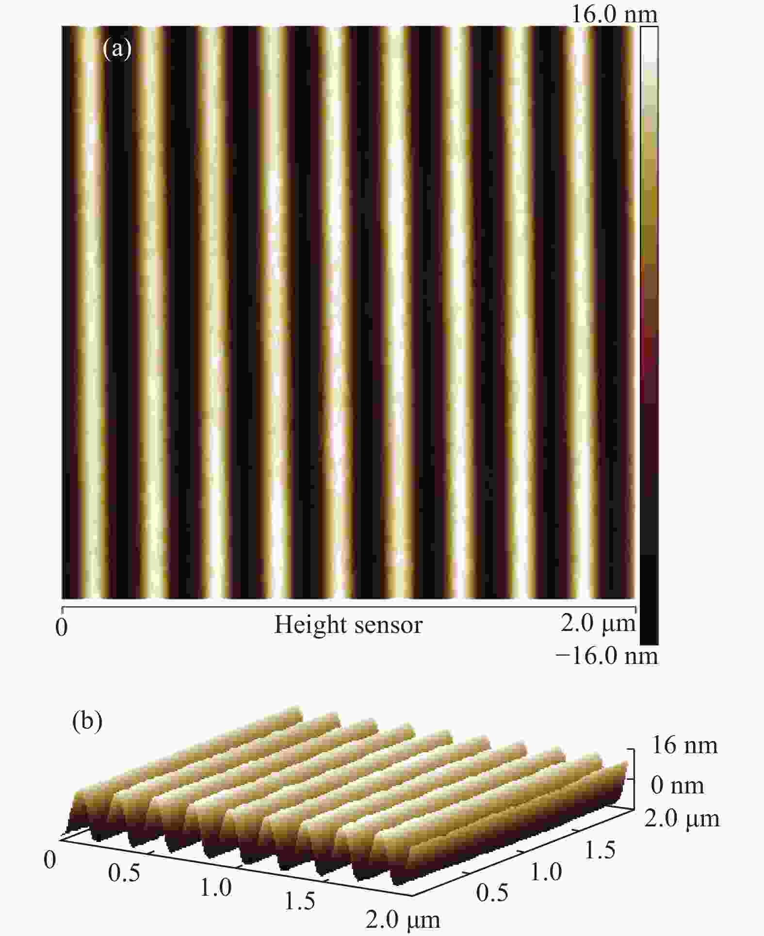
      Figure 1.  Self-traceable grating structure image. (a) 2D plane image; (b) 3D structural image

    • 在纳米技术快速发展的背景下,二维材料因凭借其在纳米尺度下丰富的光电特性受到广泛关注,并在纳米电子器件、光学和能源领域展现出独特的应用优势。二维材料中的声子极化激元具有在纳米尺度上实现光的局域和操控的能力,通过调控声子极化激元的频率,可以实现对能量的精确控制。研究声子极化激元的性质与片上光子学的发展紧密相关。在对声子极化激元进行调控的研究中,精确测量干涉条纹周期是其中一个重要方法,该方法可以直接反映调控应用效果。因此,文中构建了hBN/自溯源光栅复合结构,并利用自溯源光栅在纳米计量中的自溯源特性,同时测量自溯源光栅的周期和声子极化激元的周期,通过比对两个周期大小,基于准确的自溯源光栅周期实现对声子极化激元干涉条纹周期的精确测量,从而准确把握极化激元频率。

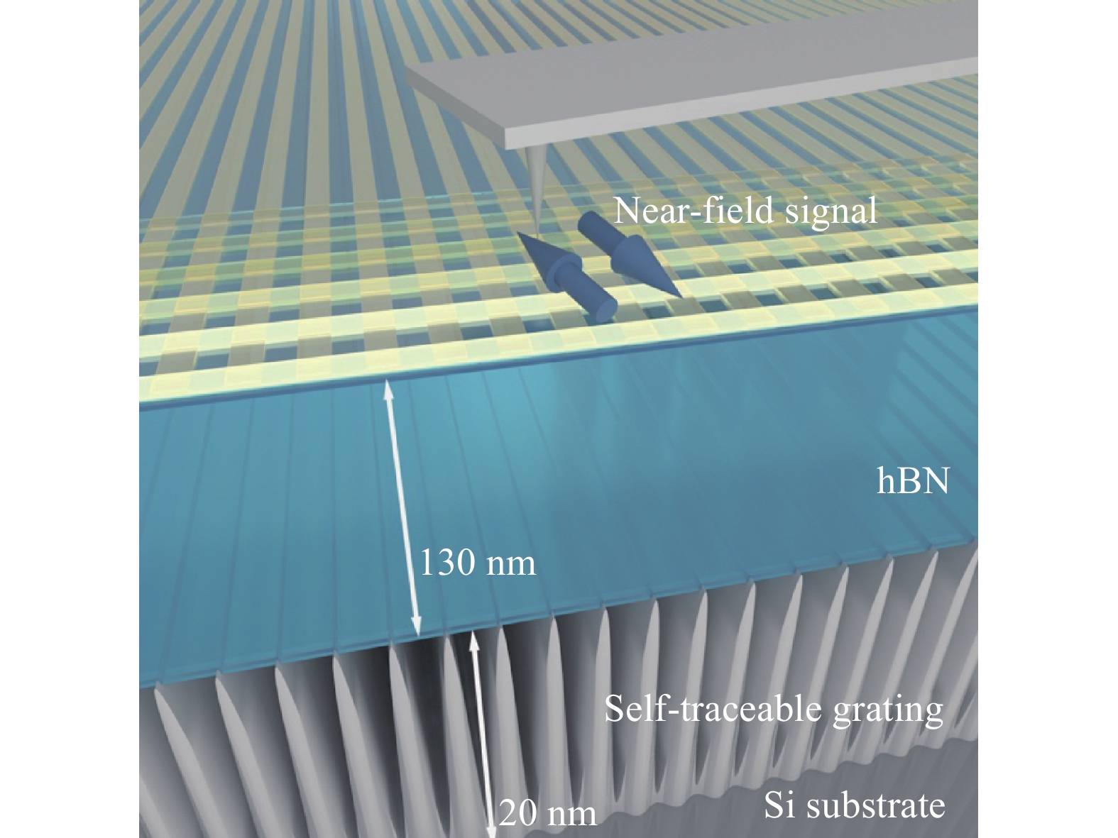
      样品结构如图2所示,其中铬光栅采用原子光刻技术沉积于硅衬底上,光栅高度为20 nm,光栅节距为212.782 nm。相邻光栅结构之间间隙为空气介质,随后,使用聚二甲基硅氧烷(PDMS)将厚度为130 nm的hBN转移至铬光栅上。对样品进行近场光学成像时,笔者将收集反向散射的近场信号(蓝色箭头),图像中会同时出现边缘极化激元激发信号,以及光栅与hBN耦合极化激元激发信号,如图3(a)所示,展现了hBN/自溯源光栅复合结构在不同位置下的纳米傅里叶红外光谱(nano-FTIR)。可以观察到随着扫描点位置的变化,近场信号强度呈现出周期性的变化,并且与光栅的周期密切相关。如图3(b)所示,蓝色线为hBN/光栅背脊的nano-FTIR光谱,橘色线为hBN/光栅沟槽的nano-FTIR光谱,在激发光波数1500 cm−1附近,光栅沟槽激发信号与背脊激发信号产生明显差异,光栅结构与hBN发生耦合效应。因此,在实验测试中,也选用激发光波数1 500 cm−1作为激发光。这种对比现象的产生可以归因于材料衬底的介电常数变化,光栅背脊处的衬底为金属铬,光栅沟槽处的衬底为空气,他们对hBN的近场信号强度具有不同的影响。基于以上原理,铬光栅-hBN复合结构的近场信号强度将呈现出周期性变化,并且变化的周期与铬原子光栅的节距一致。

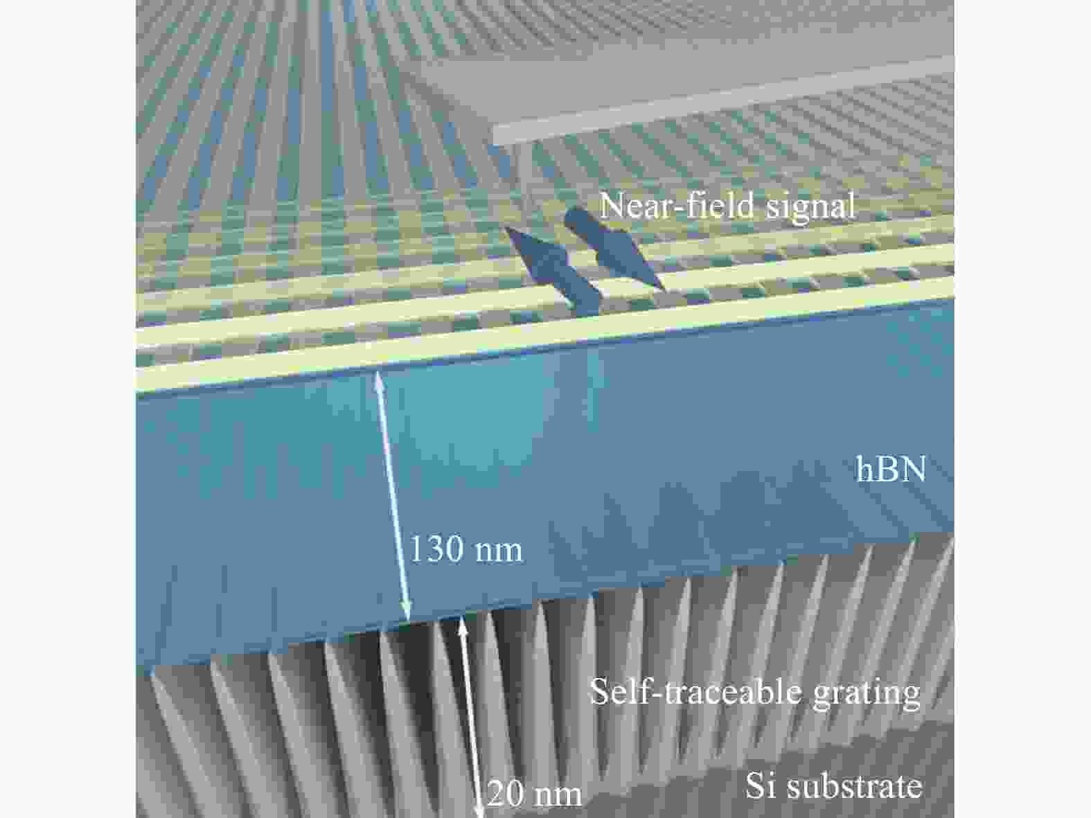
      Figure 2.  Schematic diagram of hBN/self-traceable grating structure

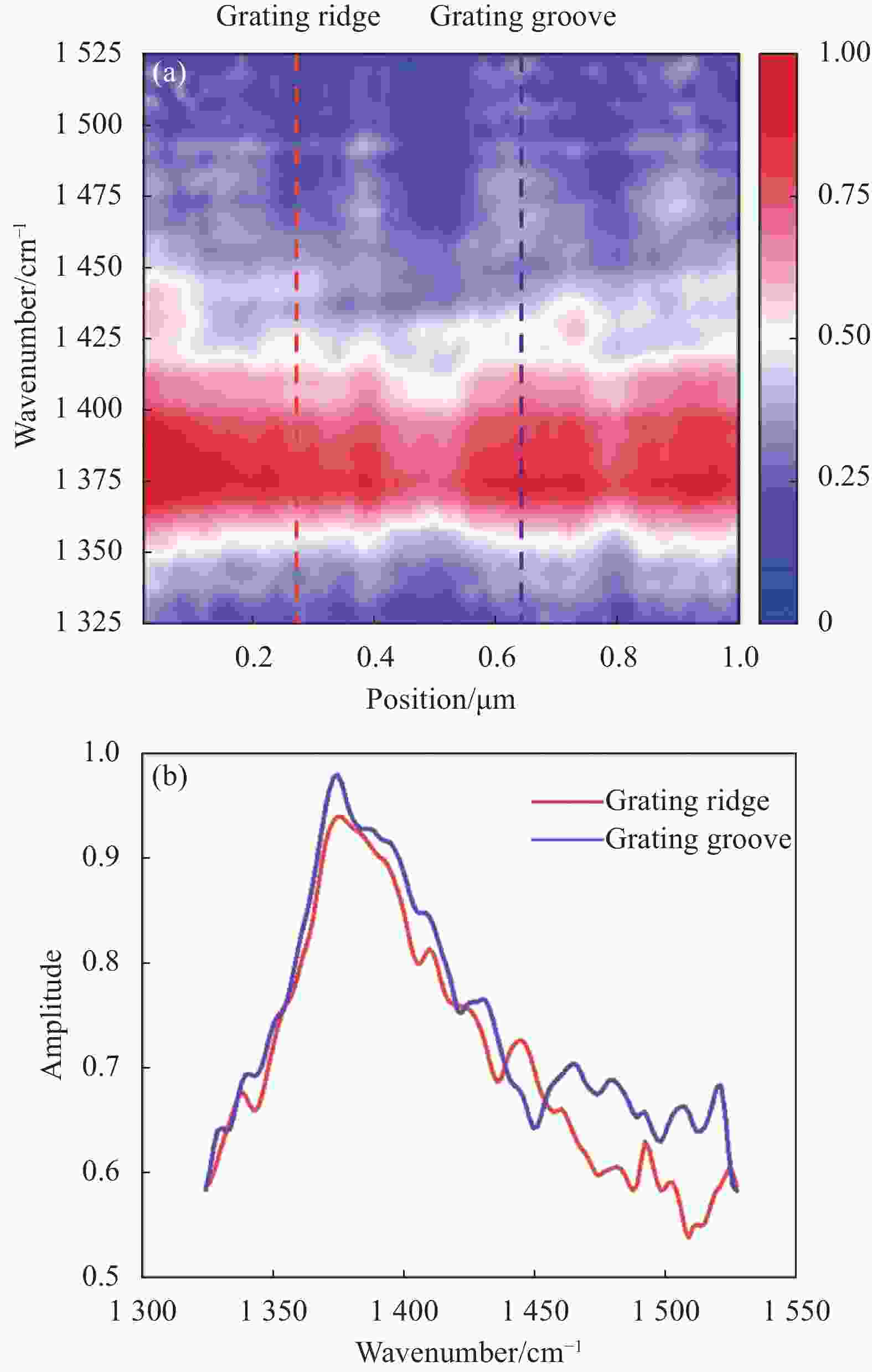
      Figure 3.  (a) nano-FTIR spectra of hBN/self-traceable grating structure; (b) nano-FTIR spectra of hBN/self-traceable grating structure at the grating ridge and grating groove

      使用散射型扫描近场光学显微镜(s-SNOM) 对复合结构的声子极化激元进行近场空间成像。样品测试设备为BRUKER公司的纳米级红外光谱仪Anasys nanoIR3-s,见图4(a)。该设备测量图像具有10 nm空间分辨率,测试中设置尖端驱动频率为240 kHz,激发光波数为1500 cm−1,收集背向散射光信号,并经过数据处理得到二阶近场信号。图4(b)为测试样品近场光学成像,图4(c)为样品表面结构AFM成像。可以观察hBN/自溯源光栅复合结构部分,呈现出周期性分布的近场信号增强条纹,该增强条纹产生在光栅沟槽处,即说明条纹间距与自溯源铬光栅节距一致,具有可溯源性。同时,PhPs的干涉条纹在材料边缘位置出现,并在靠近边缘处产生强度最强的条纹,随后的条纹强度逐渐减小,其周期表示为hBN声子极化激元波长的二分之一$ {\lambda }_{p}/2 $。声子极化激元波长$ {\lambda }_{p} $的大小受样品厚度等材料参数调控,同时反映了纳米尺度的能量传播速率等特性。因此,对干涉条纹周期的精密测量将直接反馈二维材料的光学特性。

      Figure 4.  (a) Sample testing equipment, BRUKER Company’s nanoscale infrared spectrometer Anasys nanoIR3-s, with 10 nm spatial resolution; (b) Near-field optical imaging of the sample, where the blue color represents the region of the hBN/self-traceable grating structure, and the yellow color represents the region of the self-traceable grating; (c) Atomic Force Microscopy imaging of the surface structure of the sample

    • hBN/自溯源光栅复合结构形成了对PhPs的周期性调制作用,考虑到原子光刻铬光栅的自溯源特性,使测得的PhPs近场光学图像展现出与光栅周期相符的激发增强条纹,条纹间距可溯源至铬原子跃迁频率对应波长的一半λ/2,即212.782 nm,其中光栅样品引入的测量不确定度为0.008 nm。此外,成像设备SNOM通过收集针尖和样品之间的近场相互作用散射场信号进行测量,其成像分辨率受到探针尖端曲率的限制,该实验所用SNOM分辨率为10 nm,且基于原子力显微镜(Atomic Force Microscope, AFM)搭建的SNOM无法避免扫描不同尺寸图像的过程中,电动位移台会引入的位移误差。利用AFM和SNOM对同一样品位置不同扫描范围进行了近场光学信号测量精度的对比性研究,图5(a)~(c)分别为1 µm×1 µm、5 µm×5 µm以及10 µm×10 µm不同扫描范围的AFM图像,图5(d)~(f)为对应的SNOM成像。采用图像分析软件分析干涉条纹周期以及自溯源光栅图像分析方法,对不同扫描范围的SNOM成像进行对比研究,测量结果表现出自溯源光栅对测量值精度的有效提升,见表1

      采用图像分析软件对近场显微图中干涉条纹的周期进行线性拟合,提取干涉条纹的周期数值,该图像分析软件测量精度为0.001 µm,因此使用该方法测得干涉条纹周期值保留至1 nm位数。利用该方法所得测量结果表现出,当扫描范围较小时,测量误差较大;扫描范围较大时,由于SNOM图像中有多个干涉条纹用于数据拟合,因此测量误差较小。但是,对比三种不同扫描范围,整体测量结果具有不稳定性,考虑到设备分辨率为10 nm,标准偏差值可计算为4 nm。

      自溯源光栅图像分析方法通过编写图像分析程序,对干涉条纹周期与自溯源光栅进行比对测量,以光栅周期为标尺,测定干涉条纹周期,在测量过程中,设置光栅节距大小为212.78 nm,精确至0.01 nm,因此利用该方法的测量结果保留两位小数。文中1 µm×1 µm、5 µm×5 µm以及10 µm×10 µm三种扫描范围的图像中,自溯源光栅节距值始终稳定,能够在不同扫描范围下作为稳定的标尺使用,对干涉条纹周期的测量值标准偏差为0.34 nm。与图像分析软件中数据拟合的测量方法得到的标准偏差为4 nm相比,文中提出的自溯源光栅图像分析方案将测量精度提升了一个数量级,实现了亚纳米精度的测量。为进一步降低测量偏差值,一方面可采用高度较高的自溯源光栅与hBN相结合,以提供更强的耦合信号,提升计算准确率;另一方面,在二维材料制备过程中确保边缘整齐、高度均匀,以提供分布均匀的边缘激发信号。此外,自溯源光栅的引入,不仅能够测量周期尺寸,也可对探测设备的测量位置进行校准。以该研究测试设备SNOM为例,图5(f)中已测量的条纹周期为261.41 nm,与图像分析软件拟合测量值为257 nm,因此设备位移装置应校准尺寸$ \mathrm{\Delta }U $约为−0.18 nm/pt,校准不确定度与光栅不确定度相关,具有亚纳米级准确度。然而,实际测量中仍需考虑设备分辨率对测量准确度产生的影响。仍以SNOM为例,其位移台在二维XY方向精度<0.2 nm,接近校准需求,则在实际校准中,受机械结构固有精度影响仅可在极限位移精度下完成精确校准。

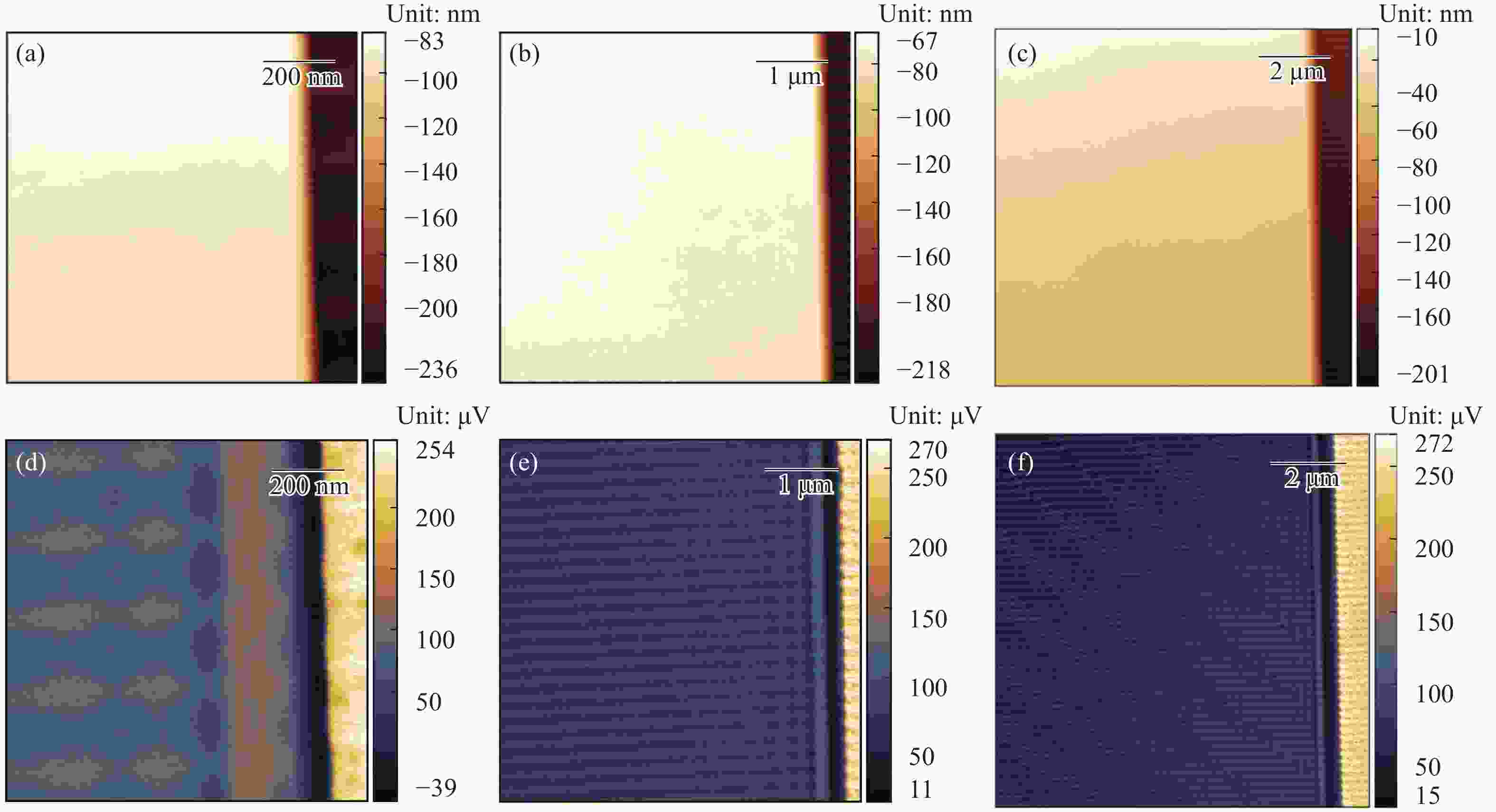
      Figure 5.  A comparative study of AFM and SNOM images of hBN/grating composite structures with different scanning ranges. (a)-(c) AFM imaging of the sample surface morphology (The imaging sizes are 1 µm×1 µm, 5 µm×5 µm, and 10 µm×10 µm, respectively); (d)-(f) Near-field optical imaging of the sample corresponding to the previous images (The imaging sizes are the same as mentioned above)

      Scanning range/µm2Image analysis and period fitting/nmImage analysis of self-traceable grating/nm
      1×1264261.28
      5×5254260.35
      10×10257261.41
      S. D.40.34

      Table 1.  Measurement of interference fringe period in images with different scanning ranges

    • 二维材料表现出的优异的光电性能,尤其是二维材料中的声子极化激元由于光场增强和低损耗率等特性,使得研究其在能量传输与控制方向的应用具有重要意义。这为光电子器件中控制载流子传输、调制光学特性等应用提供了支撑,对于未来的微纳器件制造具有深远的意义。声子极化激元的干涉条纹由红外激光与晶体光学声子耦合形成,携带材料能量传播信息,因此精确测量条纹周期可以深度分析材料在层厚、衬底、激发光等多个因素耦合下的特性。文中通过构建二维材料hBN/自溯源铬光栅的复合结构,利用hBN与衬底光栅结构变化产生的声子极化激元强度周期性变化的原理,使用扫描近场光学显微镜成像,得到复合结构表现出与自溯源光栅节距分布一致的耦合增强条纹。通过编写图像分析测量程序,将自溯源光栅条纹周期212.782 nm作为标尺,测量得到干涉条纹周期为(261.01±0.34) nm,与传统拟合测量标准偏差值4 nm相比,实现了测量精度一个数量级的提升。同时,根据测量结果可实现对设备的纳米级校准,文中对SNOM设备成像校准−0.18 nm/pt,不确定度与光栅不确定度相关。该计量测试方法为准确测定声子极化激元激发周期以及把握调控光子声子耦合,提供了准确度更好、可靠性更强的方法,同时为二维材料应用于纳米级设备的设计与调控方案提供了实验基础。

Reference (21)

Catalog

    /

    DownLoad:  Full-Size Img  PowerPoint
    Return
    Return