


-
自1960年代以来,Veselago[1]就提出了介电常数和磁导率为负的左手材料的预测。直到20世纪初,Pendry引入了超材料的概念来实现这种自然界不存在的材料[2],即由以特定形式排列的人工结构单元组成的材料可以产生异常的电磁特性,而这种特性在天然材料中是不存在的。后来,Simith等人通过实验实现了超材料的负折射现象[3]。自此,超材料的设计概念引起了广泛的关注,产生了光子晶体[4-5]、左手材料[6-7]、隐身斗篷[8-9]和其他新颖的光学器件[10-12]。但是,由于制造复杂的三维结构的挑战,很难在光学频率上实现超材料的许多潜在应用。为了解决这一难题,超构表面(超材料的二维形式)被提出并引起广泛研究,为设计光学元件的提供了新的范式。
超构表面通常由排列在二维平面中的亚波长结构(超构单元)组成。通过调整超构单元的形状、大小、方向或位置,可以在界面处引入相位梯度,并任意控制光波前。2011年,哈佛大学Capasso小组[13]首次提出了广义斯涅尔定律,并通过实验证明了V形等离激元天线在界面处形成相位不连续性导致的异常反射和折射现象。然而,由于等离激元纳米结构在光学范围内的高固有欧姆损耗,超构表面的器件的效率难以提高,这限制了它们的实际应用。因此,由高折射率的全电介质结构组成的超构表面被引入以实现具有高效率的纳米光子器件[14-18]。通过克服光吸收的关键问题,它架起了基础纳米光学与实际应用之间的桥梁。此外,超构表面的制造与互补金属氧化物半导体(CMOS)的制造过程兼容,因此实现更紧凑光学系统的广阔前景。利用亚波长尺度上光与物质相互作用,除了相位操纵外,超构表面还具有调节具有不同自由度(例如振幅[19-24]、频率[25-26]、色散[27]和偏振[28])的强大能力。因此,各种基于超构表面的应用不断涌现[29-31]。例如,在人造天线中利用电偶极子共振、磁偶极子共振或晶格共振来控制振幅,实现完美吸收体[32-33]、结构色[34- 35]、振幅型全息[36]等。超构表面用于频率调控可以实现非线性生成[37](例如二次谐波生成和高谐波生成)、光学混频器[38],光束整形[39]、非线性超构透镜[40]、非线性全息图[41]。利用偏振调控能力,可以实现偏振分束[42]、偏振成像[43]、偏振检测[44]等应用。超构表面的色散调控被应用于多波长[45]、窄带和宽带消色差[46-47]、光谱仪[48]和彩色全息图[49]。随着超构表面向功能化、器件化和集成化方向发展,超构表面如何从实验室走向实际应用成为各个领域关注的热点,这其中,超构表面的加工制造至关重要。
然而,由于超构表面是由在二维平面上高自由度、非周期性、排列密集的亚波长单元结构组成,在光学波段(从紫外、可见光到红外光波段)的超构表面更是对加工提出了很多极端的参数要求,对其走向实际应用提出了极大的挑战。比如,由于在光频段,亚波长超构单元结构要求极小尺度(如可见光波段l5~400 nm);由于在平面内调控结构尺寸实现光场调控,则需要极高精度(如可见光波段16 阶相位需要大约5 nm调控精度);为了实现足够高的工作效率,超构单元一般由难加工的高折射率的电介质材料构成,如TiO2、GaN、Si3N4、HfO2、Si等;为了实现多功能集成,如单片宽带消色差透镜等,需要极高深宽比的电介质材料的加工;为了实现大面积的超构表面元件加工,需要跨尺度(纳米到米)、高效率(TB数据量)、低成本的加工方法;为了实现纵向堆叠的集成超构表面系统,则需要纵向极高的对准精度。所以,文中将从光学波段超构表面的加工角度,总结近些年来从小批量原理验证加工到大面积量产制备探索的光学超构表面微纳加工方法的研究进展。由于超构表面加工中最关键步骤为结构图形化,所以文中将以图形化手段分章节介绍其在光学超构表面加工中的应用。首先,介绍了高自由度直写技术,如电子束、离子束、光子束直写;其次,介绍了大面积的模板转移技术如投影式光刻、纳米压印技术等,之后简要介绍了一些新兴的纳米加工技术在超构表面的应用;最后,对光学超构表面微纳加工的研究现状进行了总结并对未来发展和前景做出了展望。
-
电子束曝光(Electron Beam Lithography, EBL)是一种基本的纳米加工技术,不仅可以直接制备任意的具有亚10 nm特征尺寸的二维结构,而且还可以通过加工掩模和模板以实现后续高产量的纳米图形转移加工,所以其已是纳米加工中最重要的根技术之一。该方法的原理是通过高度聚焦的电子束对抗蚀剂进行曝光改变其在随后显影过程中的溶解度,配合后续图形转移工艺以形成设计结构。对于正性抗蚀剂在经过电子束曝光后,可被分解成更小、更易溶解的碎片,其溶解度会经历由低到高;而在负性抗蚀剂中,电子使材料发生交联反应,将较小的聚合物结合成较大的、溶解度较低的聚合物使得溶解度变低。这种直写系统具有分辨率极高的优点,并且能够在无掩模的情况下制备任意图形,缺点是在制备大面积复杂图案耗时较多,且有邻近效应的限制。为克服其缺点,研究者也尝试使用了投影式EBL技术和大规模平行电子束技术。正是由于EBL分辨率高、自由度大的特点与二维非周期性纳米结构组成的光学超构表面的加工要求非常契合,所以EBL在目前超构表面的加工中应用最为广泛。但是由于EBL必须在抗蚀剂上加工图案,而抗蚀剂多为低折射率聚合物电介质材料,一般无法直接作为超构表面单元,所以通常EBL作为图形化手段会和后续的图形转移工艺结合进行超构表面的加工,而对于金属、电介质、智能材料等又有不同的加工工艺路线,下面将分别总结。
在超构表面的发展初期,绝大多数超构表面由金属型(即等离激元型)的单元组成。此种超构表面的一般通过金属中的等离激元共振相位或几何相位进行相位调制,所以对金属厚度要求较小,其制备通常采用如图1(a)的加工工艺。首先,通过EBL方法在抗蚀剂中进行曝光,结合显影形成所需超构表面的互补图形;之后进行金属薄膜的蒸发或溅射沉积,由于该种沉积方法台阶覆盖率较差导致衬底和抗蚀剂上的金属隔离,所以可以通过剥离的方法将抗蚀剂和其上的金属去除,留下的衬底表面的金属即为所需的超构表面。该种加工方法简单且重复性高,可基本保证厚度较小的金属结构的保形性,在超构表面的小面积原理验证中非常有效,所以应用广泛。2011年,哈佛大学Capasso研究小组首次提出广义斯涅耳定律[50],在验证实验中他们设计了八个宽度220 nm、厚度50 nm的金材料V形天线在红外波段实现了0~2
$ \mathrm{\pi } $ 的透射相位调制,并利用EBL结合剥离工艺进行加工验证了异常光束偏折的效果,如图1(b)所示。该工作为超构表面设计提供了理论基础和新的范式。之后基于该相位调控原理和加工方法的等离激元型超构表面被广泛应用在不同光学波段和不同金属体系中(如银、铝、铬以及镁等),以实现光束偏折[51]、透镜聚焦[45, 52]、全息显示[53-56]、动态超构表面[57-59]等各类应用。但是由于透射型等离激元结构的固有欧姆损耗和反射损失导致该类器件透射效率较低,因此复旦大学周磊研究组通过在金超构表面下在沉积一层金反射层,并用很薄的电介质层隔开,后续工艺与上述金超构表面相同,加工了近红外波段的异常反射超构表面[60],如图1(c)所示。由于该器件消除了透射且抑制了镜面反射,因此从入射光到异常反射模式的转换效率很高(达到约80%)。并且,该器件具有宽带(750~900 nm)工作范围以及在异常反射后保持光偏振不变的性质。此工作为实现金属高效率超构表面提供了新的解决方案,基于此,国内外研究者们设计并加工了多种高效率反射型金属超构表面被应用在光束偏折[61]、多通道全息[62-67]、消色差透镜[68]、多功能超构表面[69]中。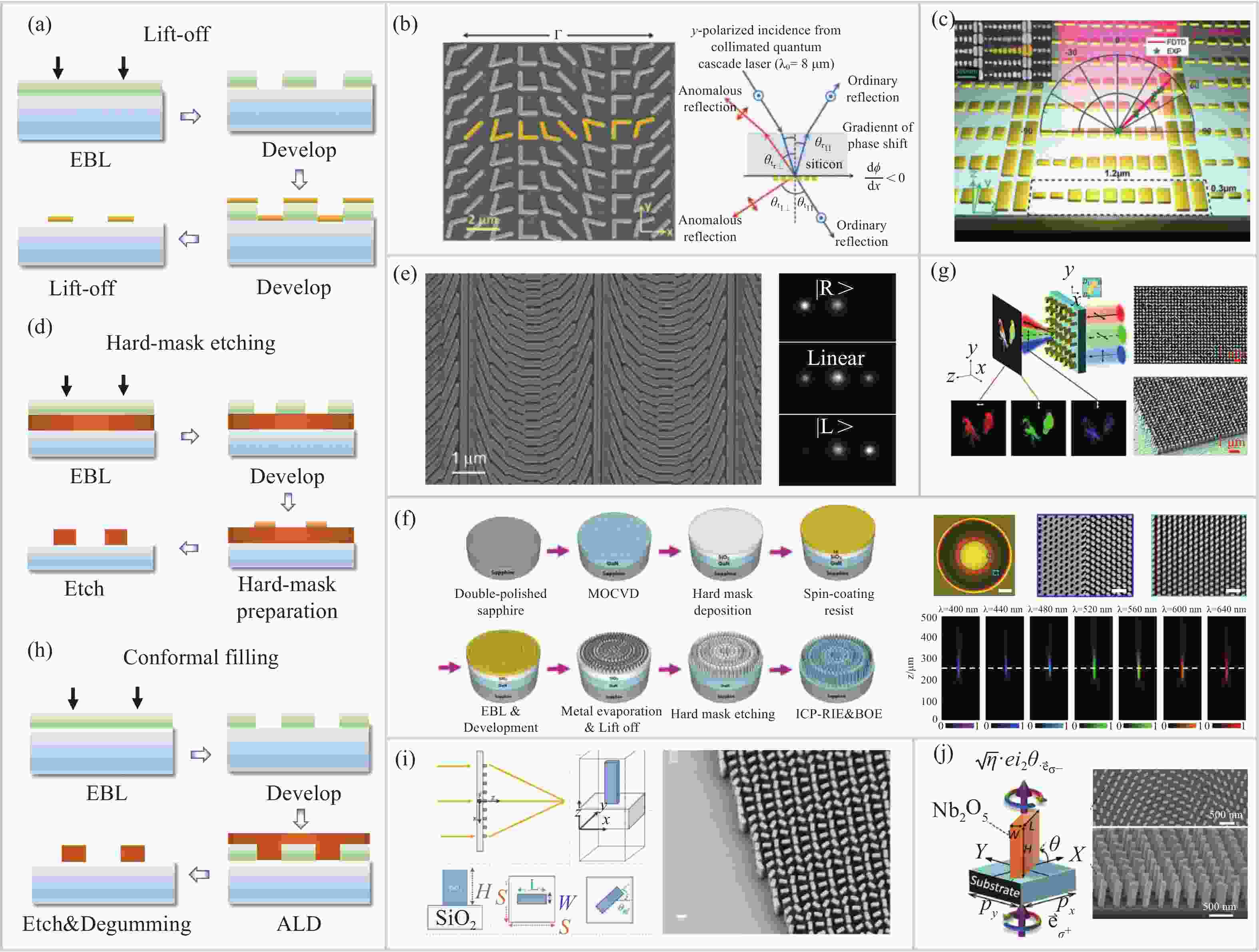
Figure 1. Fabrication of metasurfaces by electron beam lithography (EBL). (a) Lift-off process for metallic metasurfaces fabrication and its processed (b) transmissive metallic metasurface and (c) reflective metallic metasurface; (d) Hard-mask etching process for dielectric metasurfaces fabrication and its processed (e) Si metasurface, (f) GaN achromatic metalens and (g) TiO2 holographic metasurface; (h) Conformal filling process for dielectric metasurfaces fabrication and its processed (i) TiO2 metalens and (j) Nb2O5 metasurface
然而反射式光学器件的应用场景非常有限,且金属型的超构表面加工工艺和半导体工艺兼容性较差。所以,基于全电介质型的超构表面被提出,并引起广泛关注和研究。此种超构表面一般由高折射率电介质单元组成,利用与空气的高折射率对比度以在波长厚度下提供足够的相位调制。由于光与电介质材料无电子耦合震荡效应,所以基本无光损耗,可以实现高效率光学器件。另外,很多电介质材料为半导体材料,与半导体工艺兼容性较好。哈尔滨工业大学的肖淑敏和莱斯大学的Naomi Halas研究组分别探索利用上述剥离工艺对电介质超构表面进行加工,以实现全电介质结构色打印[35]和三次谐波生成[70],但是该方法仅适用于电介质结构深宽比较小且保形性要求不高的应用中。对于利用传播相位或几何相位调制的电介质超构表面,要达到足够大的相位调制和高的衍射效率,一般要求电介质的折射率较大且高度较高,因此,需要高深宽比且保形性好的电介质材料加工工艺。其中,最常用的工艺如图1(d)所示的硬掩模刻蚀工艺,即首先在目标衬底上沉积一层厚度与超构表面结构高度相同的电介质层;之后在其上进行图形化硬掩模的制备,掩模制备可以利用上述EBL结合剥离的工艺制备,也可以同样利用刻蚀工艺将抗蚀剂图案转移到掩模上;最后再利用如反应离子刻蚀(Reative Ion Etching, RIE)、电感耦合等离子刻蚀(Inductively Coupled Plasma, ICP)等干法刻蚀方法将掩模图案转移到电介质薄膜中,完成高深宽比超构表面的加工。由于干法刻蚀在半导体工艺中应用非常成熟,特别是硅材料的加工,且硅的光学折射率在可见光到红外波段都比较高,所以在电介质超构表面发展到现在,硅超构表面一直占据重要位置。2014年,斯坦福大学的Brongersma研究组[71]采用刻蚀工艺将100 nm厚的硅层图案化为密集的硅纳米天线实现了高效率超薄的波片光栅、透镜和轴锥镜,如图1(e)所示。同时期,加州理工大学Faraon研究组、哈佛大学Crozier和Capasso研究组也前后利用类似加工工艺加工了硅超构表面实现了偏振相位全调控超构表面[72]、偏振分束器[42]以及消色差光束偏折[73]。之后,基于EBL和刻蚀工艺的硅超构表面被广泛应用在红外到可见光波段的实现高效率的全息显示[74-80]、透镜成像[30, 81-85]、量子光学[86-87]、生物检测[88-91]、偏振探测[44, 92]和多功能超构表面[93-97]等各类应用中。但是由于硅在可见光波段的存在一定的光吸收影响其工作效率,研究者们又开发了其他更适用于可见光波段工作的电介质如GaN、Si2N3、TiO2的刻蚀工艺[68, 98-101],如图1(f)所示为蔡定平研究组开发的基于EBL的GaN刻蚀工艺,为了加工极高深宽比的GaN结构,他们使用一层400 nm的SiO2 作为硬掩模,加工了高度为800 nm高度的GaN超构表面以实现在可见光波段的消色差超构透镜[68]。另外,笔者与肖淑敏等人合作也利用刻蚀工艺加工了800 nm高度的TiO2超构表面实现了偏振多通道的彩色全息显示[101],如图1(g)所示。但是选择性刻蚀对于高深宽比的保形性较差,工艺较为复杂。Capasso研究组在2016提出的电介质超构透镜的工作中开发了一种基于EBL的共形填充工艺,如图1(h)所示,首先通过EBL在厚度与超构单元结构高度相同的抗蚀剂中进行图形化,之后通过原子层沉积(Atomic Layer Deposition, ALD)进行电介质材料共形填充,再通过刻蚀工艺将上层多余的介质层抛光,最后将抗蚀剂去除后则可以得到所需的电介质超构表面。此种方法由于ALD的共形性使得结构形貌直接由抗蚀剂的形貌决定,可以得到高深宽比、陡直度高电介质结构。图1(i)所示为该种工艺加工的TiO2超构透镜,可以实现在可见光波段接近衍射极限的高效率聚焦[102]。之后,Capasso研究组将该种工艺应用在透镜成像[46, 103-106]、偏振成像[43, 107]、量子光学[108-109]中。中国科学技术大学黄坤等人[110]和华中科技大学张诚[111]等人也利用该工艺加工了Nb2O5和HfO2材料实现紫外的超构表面,如图1(j)所示。最近,也有研究者尝试直接利用高折射率抗蚀剂进行超构表面的EBL加工[112],他们利用ma-N 2410负性光刻胶实现了超构表面的加工,该种方法工艺简单,但是由于折射率仍然较低,所以需要极高深宽比的抗蚀剂结构,导致结构稳定性较差。
-
聚焦离子束(Focused Ion Beam, FIB)刻蚀是目前最精确的无掩模微/纳米加工方法之一。该方法既可以通过离子束对表面的轰击将原子从表面去除,也可以通过离子轰击气相前驱体使其分解并沉积在样品表面,所以同时具备自下而上和自上而下的制造方法,这增强了FIB精确制造复杂的3D微/纳米结构的能力。另外,由于FIB无材料选择性,可以加工任何硬金属和非金属,且深宽比较大。由于可以直接去除材料,FIB加工无需后续图形转移工艺。通过集成扫描电子显微镜(Scanning Electron Microscope, SEM)、能量色散光谱和其他设备如高精度压电台、微/纳米机械手等,FIB成为了一种自由度极高且可实时观测的微/纳米加工技术。但是,FIB成本高、加工效率非常低、且加工的基底尺寸有限,限制了其只能在制样、修复和小批量原型验证等应用,另外,由于一般的Ga+束流直径要比电子束流大,所以分辨率比EBL低。利用其自由度大的特点,FIB加工方法在超构表面的小面积原理验证方面有广泛的应用。
Ni等人[113]首次通过FIB直接刻蚀金薄膜材料加工了V形孔状结构全息超构表面,如图2(a)所示,其厚度仅为30 nm。该超构表面可以在可见光波长范围内提供二阶振幅和八阶相位复合调制,从而生成高分辨率的低噪声全息图像。之后,类似的FIB加工孔型结构的相位调控也被用在实现超构透镜[48]、彩色全息[114-115]、电控光束偏折[116]、涡旋光生成[74, 117-119]、非线性超构表面[120]等各类功能中。FIB孔型结构也常被用来实现近场光波操控的超构表面[121-122],如Lin等人[121]利用两个垂直亚波长金狭缝单元的阵列实现表面等离激元的偏振可调定向传输,并保留入射光的偏振信息,如图2(b)所示。此外,该类结构也被Cheng等人[123]应用在结构色打印超构表面中,他们采用了一种薄层金属−介电−金属(MIM)结构,通过在上层银膜上加工周期性孔阵列的完美吸收体,通过简单地调整孔的大小和周期即可调整吸收峰,可在整个可见光频率范围内定制具有高品质因子的吸收共振,如图2(c)所示。除了孔型结构以外,如果在FIB加工过程中将所需结构的外围材料进行刻蚀,聚焦离子束也可以加工纳米柱形结构[124-125]。Ma等人[124]通过此种方法加工了几何相位型的银纳米天线超构表面,如图2(d)所示。该超构表面具有两个主要功能,首先,对于圆偏振入射光束,超构表面将其转换为承载轨道角动量的涡旋光束,其次,入射场可以聚焦成具有一定焦深的点。FIB高自由度的特点也赋予其(准)三维结构的加工能力,如Chen等人[126]通过预先编辑的bmp灰度图控制不同的离子剂量可以实现不同深度的金纳米缝隙和凹槽,如图2(e)所示。该种独特设计可以在向前方向上将特定方向的入射圆偏振光转换为指定的线性偏振光,而在向后的方向上选择性地将某个线性偏振分量转换为所需的圆偏振光。而通过纳米折纸技术,Liu等人[127]展示了基于悬浮的超薄金膜的FIB诱导的连续形状变换,可以容易地制造具有宽带偏振转换和敏感的相位特性的风车状三维超构表面。通过故意用相反的手性周期排列超构表面单元,可以在线性和径向构型下成功观察到高对比度的交叉极化衍射。

Figure 2. Fabrication of metasurfaces by focused ion beam (FIB) etching. The metallic nano-hole structures fabricated by FIB is used for (a) holographic metasurface, (b) near-field light field control and (c) structural color modulation; (d) Metallic nanopillar-type metasurface etched by FIB for vortex optical focusing; (e) Metasurface of quasi-3D structure fabricated by FIB. Non-metallic metasurface fabricated by FIB, such as (f) GST phase change material metasurface, (g) perovskite metasurface and (h) metal-dielectric multi-material laminated structure
FIB加工方法由于无材料选择性的优势,也被用在除金属外的其他各类难加工介电材料中[128-132]。Karvounis等人[128]利用相变介质碲化锗锑(GST)中的非易失性、非晶态/晶态转变来实现可光转换的全介电超材料,如图2(f)所示。通过FIB刻蚀出 GST纳米光栅结构呈现出高质量的共振,该共振通过激光诱导结构相变在光谱上发生了位移,从而在可见/近红外波长下提供高达5∶1 (7 dB)的反射率和透射率之比切换对比度。Gholipour等人[129]通过FIB加工高折射率低损耗的金属卤化物钙钛矿纳米光栅或纳米狭缝,通过改变纳米结构的几何参数第一次实现了可调的高Q因子共振的彩色钙钛矿超构表面,如图2(g)所示。更进一步地,FIB也可以加工由多层不同材料构成的超构表面[130],如图2(h)所示,Smalley等人设计并加工了一种发光双曲超构表面,其由InGaAsP半导体多量子阱(MQW)和Ag膜多层交叠构成并被FIB加工成亚波长光栅结构,MQW充当与Ag结合的发射源和组成电介质,其可以同时实现最佳的光与物质相互作用并抵消材料损耗。
-
激光直写加工技术(Direct Laser Writing, DLW)利用激光束对材料直接扫描加工,从而改变材料的物理化学性质,比如折射率、消光系数、带隙、电导率和表面浸润特性(亲水性或疏水性)等,拥有无掩模、自由度高和成本低的优势。根据直写中不同的材料加工机理,DLW又可以分为连续激光直写光刻、超快激光直写刻蚀和双(多)光子聚合打印技术。但是,DLW的加工分辨率受到光学衍射极限的限制,对光学超构表面的应用限制在红外到太赫兹波段。利用双(多)光子聚合的非线性效应可以进一步的增加分辨率到百纳米,且可以实现3D打印,是未来光学超构表面集成的一种可能加工技术。此小节将对这三种DLW技术在超构表面中的应用进展进行总结。
激光直写光刻是利用强度可变的激光光束对基片表面的光敏材料实施扫描曝光,通过显影在材料表面形成所要求的图形,可再经过刻蚀沉积等薄膜工艺将设计的图形转移到基片上。Komlenok等人[133]利用激光直写光刻一步式制备的任意复杂的金刚石改性石墨化的偏振器,这种方式制备的超构表面在可见光和红外波段,具有与理论模拟的金刚石超构表面的电磁响应较好的一致性,这种金刚石改性方法非常灵活,为激光直写技术制备的全碳超材料光学元件提供了理论依据。Yan等人[134]利用一步式激光直写光刻也在中红外波段范围实现了一种偏振可控的光涡旋调制的全硅超构表面,如图3(a)所示,相比于传统的光涡旋调制器件,激光直写光刻加工的超构器件具有小型化、集成化和易于设计制造的优点。

Figure 3. Fabrication of metasurfaces by direct laser writing (DLW). (a) Polarization-controllable optical vortex modulation all-dielectric metasurface based on DLW; (b) Schematic diagram of single-step ultrafast laser interference direct writing etching process; (c) Fourier hologram based on ultrafast femtosecond laser etching technology; (d) Two terahertz metasurface with elliptic apertures fabricated by the femtosecond laser slit space control technology on the gold film; (e) 2D perovskite lens fabricated by femtosecond laser; (f) Physical image and SEM image of the new type flat lens whose performance is easy to control based on 2D perovskite nanosheets; (g) SEM images of direct and inverted photonic structure with different symmetry fabricated by two-photon polymerization 3D printing process; (h) Processing principle diagram and SEM image of the nearly perfect infrared spectrum absorption metasurface based on two-photon polymerization 3D printing process; (i) Process flow chart of computer-generated holographic projection based on two-photon polymerization 3D printing process and the schematic diagram of the hologram; (j) Schematic diagram of a Daman grating generating an N×N dot array in the far field based on two-photon polymerization 3D printing process
超快激光直写刻蚀是飞秒量级超短脉冲能量在空间中被紧聚焦之后,通过材料双光子吸收引发光聚合,可将加工区域限制在焦点中心位置,在作用区域引发物理化学性能变化,通过控制光束扫描实现二维或三维成型加工。而且超短脉冲与材料作用时间远低于材料热弛豫,超快激光直写刻蚀避免了光热效应,其独特的三维处理能力、任意形状的灵活设计、热效应最小性、损伤阈值低等特点,使超快激光可用于制作高性能、可集成、灵活便携的多功能、高精度分辨率器件。
Berzins等人[135]为了解决激光直写光刻的效率限制在脉冲激光的频率的问题,即每个激光脉冲只产生一个单一的超构表面单元,利用单脉冲激光干涉,一步式制作亚微米周期的半球形硅基Mie共振超构表面,如图3(b)所示,在可见光和红外范围内通过控制激光照射条件和初始膜厚,可以在几百纳米范围内调整其尺寸,证明了单脉冲激光干涉是一种直接且高产量效益的电介质超构表面技术。He等人[136]通过飞秒超快激光直写在熔融的石英玻璃上刻写亚波长尺度上尺寸变化的纳米凹槽,在可见光范围内实现了一种简单紧凑的电介质超构表面转换器,通过控制光轴在介质超构表面的局部方向,可以实现任意高阶激光模式。Drevinskas等人[137]也在可见光范围内利用飞秒超快激光直写技术实现包括偏振光栅、傅里叶全息图、微透镜和光学涡旋微转换器的电介质层几何相位操纵,保证了亚波长的分辨率,并提高了相位梯度,如图3(c)所示。而Li等人[138]利用飞秒激光的狭缝空间调制技术在金薄膜上制造了两种太赫兹超构表面,如图3(d)所示,定量研究了椭圆孔径的形状与加工参数的关系,包括取向角、狭缝宽度和激光脉冲能量。制备的超构表面均具有良好的多通道全息成像能力,提高了超构表面全息图的信息存储能力和加密安全性。此外,超快飞秒激光刻蚀还被用于基于二维钙钛矿纳米片上制作的性能易调整新型平面透镜[139]、基于硅基玻璃衬底制造变尺寸纳米沟槽的一种新型压电陶瓷等[140],如图3(e)~(f)所示。
双(多)光子聚合打印是利用材料双(多)光子吸收的特性,以实现光敏材料内部的任意区域的聚合[141-142]。双光子聚合是一种能够实现亚微米尺度和纳米尺度结构制造的按量(in-volume)技术,不像其他高分辨微纳制造技术如EBL受限于表面效应。双光子吸收是一种非线性现象,且双光子吸收率与入射光的强度的平方成正比,如果辐照足够高并且在基态和激发态之间的跃迁能与两个光子的结合能相匹配,任何材料都能发生双光子吸收。因此,双光子聚合打印拥有材料穿透性好、空间选择性高、三维结构高分辨率的特点。然而,虽然双光子激聚合3D打印技术在微纳尺度加工领域具有极大的优势,但并非全无缺点。例如与胶片拍摄图像类似,应用双光子聚合技术的光敏材料需要进行显影和定影等过程,从而将打印的3D物体固定下来,因此加工过程更为繁琐。Rybin等人[143] 基于双光子光刻技术加工了一组正交C2v晶格对称的各向异性样品,从实验和理论上证明了在波长530 nm光子晶体从多阶衍射模式向只有零阶衍射的模式的转变,如图3(g)所示。Faniayeu等人[144]为了解决传统光刻工艺中亚微米尺度复杂的三维结构难以加工的问题,利用双光子聚合技术和金属化处理快速设计制造了接近完美的红外光谱吸收材料超构表面,而不受平面方法的限制,如图3(h)所示。Wang等人[145]为了加工顶部刻截面的高精度三维复杂结构,如图3(i)所示,利用双光子光刻技术,通过计算机生成的全息图在相位板上的每个相位结构单元上添加顶部的刻截面,产生了不受零阶光斑和阴影影响的远场投影,同时保持了高达86%的衍射效率。此外,基于双光子光刻技术Wang等人[146]又通过使用集总双光子光刻参数模型和一系列解决方案模式来实现精确的3D打印,如图3(j)所示。通过优化参数包括激光功率、光束扫描速度、阴影距离和切片距离,加工了接近完美的毫米级达曼光栅,测量的衍射效率接近理论极限,激光光斑阵列的非均匀性低至1.4%,零阶光斑的功率比低至0.4%。
-
EBL和FIB等直写技术已经被用来制作各种功能的光学超构表面,然而它们是通过逐点扫描的方法加工,对于制备大规模的纳米结构需要大量的加工时间和较高的加工成本,因此不适合大规模生产。与之相比,投影式光刻技术(Projection Photolithography, PPL)是借助光刻胶将掩模板上的几何图案转移到基片上的技术。其中紫外光以步进或扫描的方式通过掩模板照射在表面有光刻胶的基片上,光刻胶被曝光的区域发生化学反应,通过显影技术除去曝光区域(正胶)或未曝光区域(负胶)的光刻胶,再利用刻蚀技术在基片上加工出图形,有效地缩短了曝光时间。因此,掩模光刻技术是最适合批量生产大面积光学超构表面的技术之一,有希望将光学超构表面器件从实验室走向量产应用。但是,由于光学波段的结构尺寸较小,普通的紫外光刻满足不了,需要借助半导体制程中更短波长和更先进的浸没式曝光系统,其自由度较低,成本较高,且需要EBL等手段进行掩模的制备。
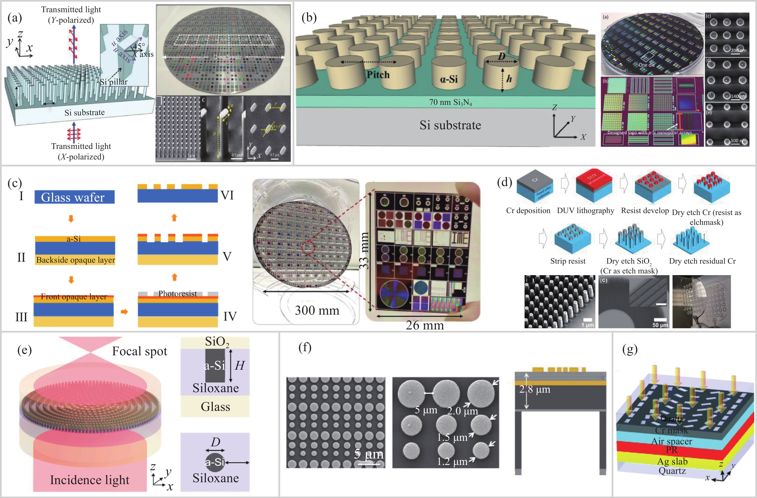
光刻技术中最常用的为非接触式投影式曝光,即图形经过光学系统成像缩放在光刻胶上,常用的是在曝光镜头与光刻胶之间充满液体的浸没式光刻,这种光刻方式,增大了分辨率,对准精度高,可以缩放掩模板上的图案,目前已经被用于加工各种基底的超构表面上。首先,光刻技术在半导体加工中是基于硅晶片设计的加工工艺,所以最简单直接的方案是直接在硅晶片上进行光刻,用于红外波长光的调制[147-150]。如Dong等人[147]在12 in (1 in=2.54 cm)的硅晶片上用深紫外光刻技术制造出了半波片,图4(a)中左图显示了半波片工作示意图,右图为电子显微镜下的图像,其高宽比超过了10∶1,晶片级器件的偏振转换效率高达95.6%。为了减小结构的高度,在基底与纳米结构之间加一层折射率低的电介质层[148, 150],这样可以增大折射率对比度。如图4(b)所示,Hu等人[148]在硅晶片上先沉积SiN和非晶硅,之后再用193 nm深紫外浸没式光刻在12 in的非晶硅上制作出了彩色显示的超构表面,其关键尺寸在100 nm以下,高度130 nm,通过控制圆柱体的直径和单元的周期尺寸,共振波长也能很好地控制。除了用硅晶片做基底,用透明的基底玻璃或者石英的工艺也被研发出来,同样包括直接在玻璃上光刻[151-152],如Zhong等人[152]开发了一种直接在12 in的石英上使用浸没式光刻的工艺来加工超构表面,为了概念证明,设计制造了适用波长为940 nm直径8 mm的超构透镜。图4(c)左侧显示了制造的工艺流程,通过在上表面沉积一层不透明层来使光刻更好地集中在前表面。光刻之后,再去掉上面与下面的不透明层。右侧显示了加工出来的12寸玻璃晶片,左下角为8 mm超构透镜。对于可见光波段,需要更小的结构尺寸,Park等人[153]使用深紫外投影步进光刻技术,在4 inch的石英晶片上制作出了45个直径1 cm的超构透镜,在633 nm波长的光下,对任何均匀的偏振光都能有良好的聚焦效果。其中晶片的照片如图4(d)所示,上边一行为光刻的流程示意图,先在铬上进行光刻,再以铬为掩模板再次刻蚀,最终得到全石英的超构表面。使用玻璃基底除了直接刻蚀,还有层转移的工艺,Hu等人[150]在12 in的石英晶片上加工出940 nm波长的超构透镜,数值孔径(Numerical Aperture, NA)为0.496。如图4(e)所示,左侧为结构单元示意图,其制作工艺为,先在硅晶片上沉积二氧化硅和非晶硅,光刻之后,旋涂胶并粘合在12 in的石英片上,之后经过抛光和刻蚀去掉下面的硅晶片,从而将图案从硅上转移到石英上。而右图则为加工后的石英晶片图片。除了透射型超构表面,反射型超构表面也可以使用光刻工艺,即在二氧化硅基底下沉积一层金属膜,如图4(f)所示,Roy等人[154]设计制造了一个金属超构透镜,在有着200 nm厚的金膜的二氧化硅背面制造了50 nm高的金纳米柱,并且与微机电系统集成,形成动态的超构透镜。

Figure 4. Fabrication of metasurfaces by mask photolithography process. (a) Schematic of metasurface-based half-wave plate by processing directly on Si wafer (left), photograph of the fabricated 12-in Si metasurface wafer and three SEM images of Si pillar array inside the center white squares of the wafer(right); (b) Schematic of color display metasurface by adding a dielectric layer before the photolithography (left), silicon wafers and nanostructures of different sizes, the bottom left is the pattern of color display (right); (c) Flow diagram of photolithography on the transparent glass substrate (left), the fabricated wafer and the enlarged unit pattern(right); (d) Lithography process of the all-glass metasurface with opaque layer (up), the SEM images of the fabricated nanopillars and result of lens(down); (e) Schematic of the metalens by layer transfer technology on glass substrate (left), the schematic of unit structure (right); (f) SEM image of reflective metasurface with a metal layer (left), the schematic of structure of photolithography (right); (g) Schematic of the near-field lithography structure with the reflective plasmonic lens
传统投影式曝光系统受到衍射极限的限制,需要短波长光源和复杂光学系统才能实现纳米级图形加工。中国科学院成都光电技术研究所罗先刚团队[155]提出了一种接触式利用表面等离激元光刻方法,具有加工效率高、分辨率高的优点,但图案大小只能与掩模板大小相同,而且掩模版容易被污染寿命较低,另外由于消逝波衰减的特点,曝光的光刻胶深度较浅并且保真度不高。基于此,他们又通过引入反射等离子体透镜来放大和补偿消逝波,具有高保真度、对比度和比以前近场光刻更深的深度。再通过刻蚀工艺将图形转移到下面的金属层上,并且具有很好的聚焦性能。其光刻结构示意图如图4(g)所示。此外该研究团队[156]还开发了另外一种近场曝光的方式,利用了等离子腔的方式增大消逝波,有效地调整了成像面的电场分量,最终加工出几何相位的全息超构表面,成功显示出字母E的图案。
-
纳米压印技术(Nanoimprint Lithography, NIL)是一种利用机械变形复制纳米结构的技术。具有高分辨率、大面积加工、低成本的优点,但是仍然需要高分辨率的设备制造模板,而且需要用刻蚀去掉压印后的残胶,对胶起到一定破坏作用。
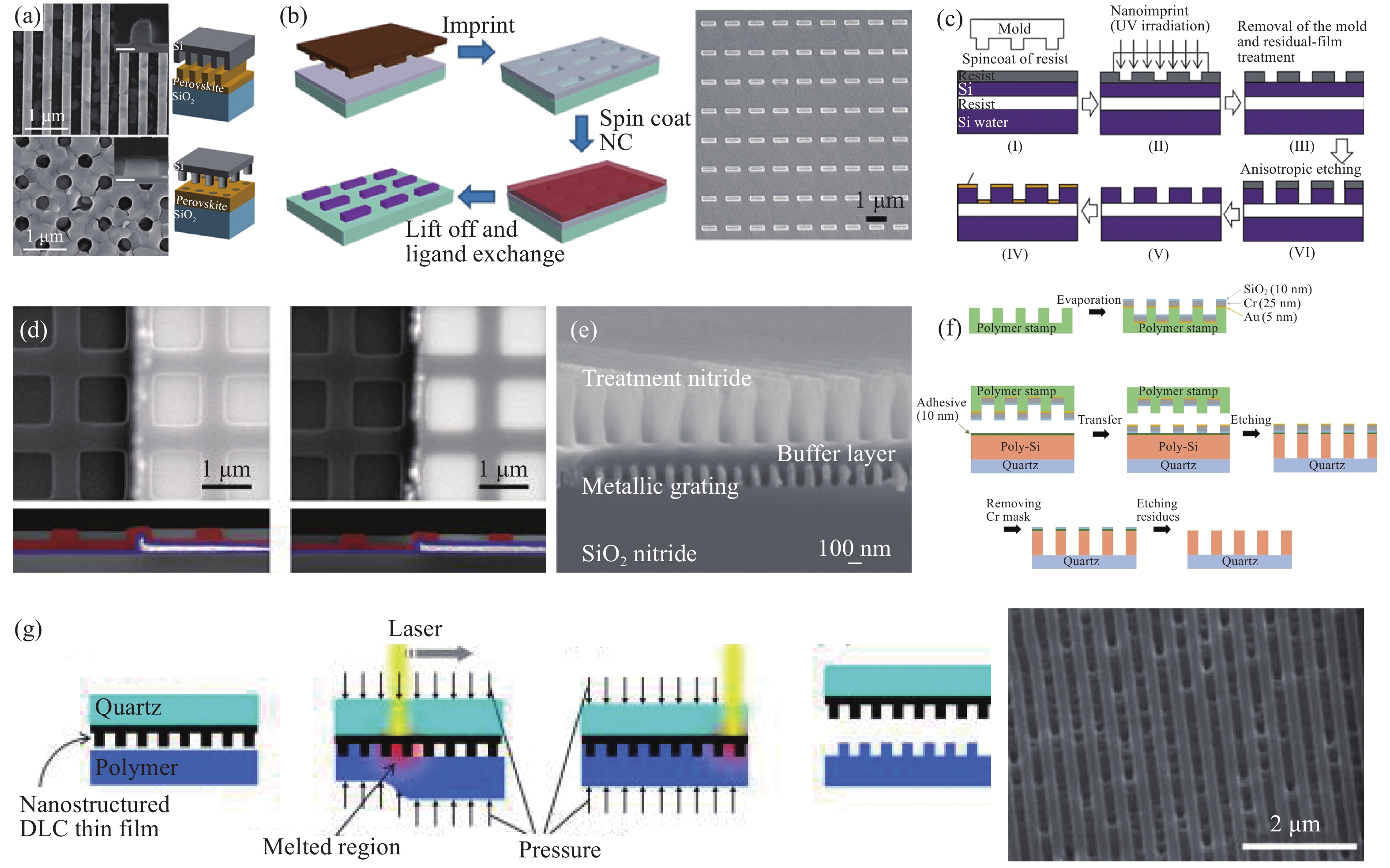
传统的NIL分为热固化和紫外光固化,热固化利用材料高温下粘度低的特点,当主模被压在基板上后,用先加热再冷却的的方式固化聚合物涂层并分离模板,NIL的图案就转移到了聚合物层。这种工艺十分简单,可以直接用于超构表面的加工[157-159],如Makarov等人[157]做出了一种光增强超构表面,利用NIL技术在钙钛矿材料上进行压印,其加工效果的显微图如图5(a)所示,分别为纳米柱与纳米孔结构,这种光增强膜可以增强光达70倍并且拥有较好的稳定性,为光电器件制备提供了一种方案。图5(b)显示了一种常见的利用NIL加工的方案[158],在压印之后旋涂胶体形态的金属纳米晶体,最后用剥离工艺去除多余材料,制作出了波片功能的等离子体超构表面,在近红外到中红外都具有高的偏振转换效率。

Figure 5. Fabrication of metasurfaces by nanoimprint lithography. (a) SEM images of the two kinds of metasurface by thermal curing nanoimprint(left), schematic of the corresponding process(right); (b) Process of manufacturing with the thermal curing nanoimprint lithography and lift off (left) and the SEM image of the fabricated metasurface (right); (c) Schematic of the UV curing nanoimprint lithography process; (d) SEM image of the fabricated thermal emission metasurface by UV curing nanoimprint lithography. Top views and cross-sectional views are showed up and down and the images of before and after removing residual glue are showed left and right; (e) Cross-sectional SEM image of the asymmetric transmission metasurface processed by UV curing nanoimprint lithography; (f) Schematic of the stamp type nanoimprints: the preparation of the nanostamp, and the imprinting of the stamp and follow-up etching; (g) Process of the laser-assisted nanoimprint and the SEM image of the fabricated metasurface
NIL的另一种固化方式为紫外光固化,使用液态的聚合物旋涂在基底上,在压印时使用紫外光辐射固化聚合物,因此模板需要对紫外光透明。这种方法省去了加热和冷却的时间,提高了生产效率,可以在室温低压的条件下进行压印。其一般的工艺流程图如图5(c)所示[160]。Miyazaki等人利用紫外光NIL制造了用于红外光二氧化碳传感的热发射器超构表面[161],图5(d)显示了压印后,残余胶去除前后的的显微图像。这种热发射超构表面对二氧化碳检测具有完美的辐射能力,可以节省31%的电量,几乎可以商业化。图5(e)显示了一种用紫外光NIL制造的具有高度不对称透射率的超构表面的横截面显微图像[162],这种超构表面在可见光到红外光都可使用,x偏振光可以从顶部全部通过,而y偏振光从底部几乎不能透过。
用于加工超构表面的NIL除了使用液相的聚合物固化的方式,还可以直接像印章一样转移固体的纳米结构,用于后面的刻蚀掩模板。如Lee等人[163],采用了如图5(f)所示的工艺制造超构表面,在基底和硅的上面沉积一层粘合层用来粘合模板上面的铬,再通过后续的刻蚀得到最终的超构表面。这种超构表面作为透明的超构透镜用于增强现实近眼显示,具有大视场高数值孔径,大孔径和宽带的特性,已经被作者用来彩色成像,可以看出NIL让超构表面的实际应用显示出了巨大潜力。
此外NIL还可以通过电力[164]或者激光等方式使材料产生变化,达到压印的目的。如图5(g)中左图显示了一种激光辅助的超构表面加工方法[165]。通过在模板背面照射激光使模板的金属表面加热从而融化聚合物,实现形状的复制。这种方法可以用较低的热量在较短的时间内大面积制造。其加工出样品的显微图显示在图5(g)右图中。
-
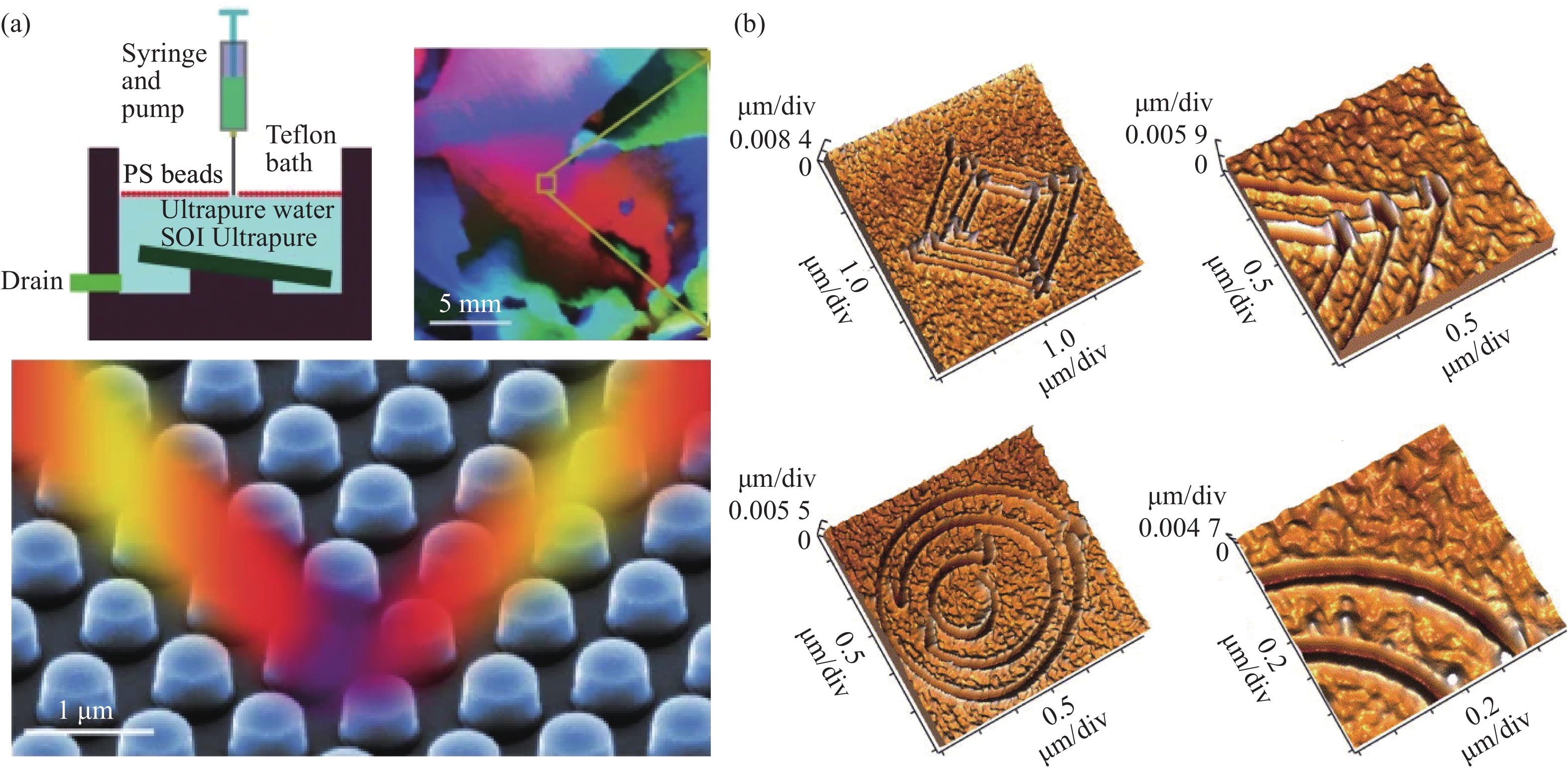
对于大面积加工超构表面,自组装技术(Self-assembly Lithography, SAL)方案也是一种高效便捷的加工方式,这种方法将胶体自组装形成的聚苯乙烯球体阵列作为掩模板与后续的刻蚀或沉积的工序结合,具有简单、低成本的优点,但是只能加工周期排列的简单图形。如图6(a)中显示的,作者利用上面所说的方法,在空气与水的交界面进行自组装,之后慢慢地将水抽出,使聚苯乙烯球体转移到水下绝缘体之上的硅基底上,用这种方法作者制作出了几乎完美的反射镜,对于波长为1530 nm的光有着99.7%的反射率[166]。为了克服传统的自组装只能加工简单周期图案的限制,研究人员还开发了其他更复杂的工序。如从多个角度沉积多次刻蚀的方法[167],还有利用两层聚苯乙烯球体堆叠作为掩模的方法[155]等。

Figure 6. Fabrication of metasurfaces by other emerging processing methods. (a) Schematic diagram of the self-assembly process (top) and the micrograph of the metasurface of the processed reflector (bottom); (b) Image of the metasurface processed by the scanning probe lithography under the atomic force microscope. The coordinate axes are x, y, z coordinates
探针扫描光刻(Scanning Probe Lithography, SPL)也是一种可以制造超构表面的纳米加工方法,这种方法利用探针移除抗蚀剂上的粒子或者排列图案中的粒子实现加工的目的,其精度由原子力显微镜控制。如图6(b)中显示了用探针扫描加工的超构表面的原子力显微镜测量图[168]。这项工作使用探针加工出80~120 nm宽4~80 nm深的沟槽,形成开口环形状的谐振体,在中红外波段实现了负折射率。从中也可看出探针扫描方法的局限,存在加工效率低、沟槽尺寸较浅较宽的问题。
-
具有光学多参量调控能力的光学超构表面可以任意构造近场和远场光波,已经成为基础研究和应用研究的理想平台。相对于传统光学元件,超构表面具有超轻、超薄及多功能集成的优势,且全电介质型超构表面效率高、加工与CMOS工艺兼容,这使得超构表面有望成为继折射光学元件和衍射光学元件的第三代新型光学元件,革新整个光学领域的面貌。然而,要真正实现光学超构表面从实验室走向实际应用,高分辨率、高精度、高深宽比、难加工材料、大面积、低成本的微纳结构的加工是关键。所以,文中总结了超构表面发展大概十年时间内的各类微纳加工方法及其在光学超构表面的应用,包括适用于小批量原理验证的直写类加工技术,如电子束、离子束、光子束直写,以及模板转移技术,包括投影式光刻、纳米压印等技术,还有一些新兴的纳米加工技术,如探针扫描和自组装技术。笔者等将这些方法的加工尺度、精度、适用波段和技术特点总结在表1中,这些加工方法各有优劣,其应用让光学超构表面得到迅速发展,但是距离超构表面的真正走向实际工程应用,仍然有很多问题需要解决。笔者等总结了以下几点光学超构表面加工方面的挑战和未来的发展趋势。
Process Feature size Applicable band Precision Process characteristics Direct
writing technologyElectron beam lithography <10 nm UV to infrared ~1 nm High resolution, high degree of freedom, low efficiency for large-scale or complicated pattern, subsequent pattern transfer process required Focused ion beam etching ~20 nm Visible to infrared <100 nm High resolution, high degree of freedom, no material selectivity, ultralow efficiency Laser direct writing ~1 μm Visible to terahertz <1 μm High degree of freedom, resolution is limited by the optical diffraction limit, subsequent pattern transfer process required Ultrafast direct laser etching <200 nm <100 nm No material selectivity, minimal thermal effect, low-damage-threshold Two-photon (multiphoton) lithography <200 nm <100 nm Higher resolution than single photon lithography, high spatial selectivity, three-dimensional structures processing Scanning probe lithography <10 nm Visible to infrared <10 nm Simple process, low efficiency Template transfer technology Immersion lithography <100 nm Visible to infrared <100 nm High resolution, high alignment accuracy, high equipment cost, high requirements of processing Plasmonic lithography ~100 nm Visible to infrared <100 nm High-resolution, high processing efficiency, short working life, poor fidelity Hot embossing Depend on the master - - Relatively simple process, time consuming which is not suitable for mass production UV-curable nanoimprint lithography Nanoscale High efficiency, material selectivity Laser assisted direct imprint ~10 nm High-resolution, low heat release during processing, short processing time Micro-contact printing <100 nm Low cost, suitable for large-area or simple pattern processing Self-assembly lithography nm - μm - ~1 nm Low cost, suitable for large-area or simple pattern processing, simple process Table 1. Summary of fabrication methods of metasurfaces and their process characteristics
(1)目前的光学超构表面加工大部分集中在新原理、新功能的验证,但是加工的器件性能和仿真差距很大。这是由于目前的加工中很少考虑材料本征特性误差、尺寸误差、形状误差、超构单元倒塌缺失等一系列加工误差引起的性能下降。如果要实现超构表面真正走向应用,则需要系统研究加工误差与器件性能之间的定量关系,建立微纳加工误差评价体系和标准以指导超构表面产业化生产;需要研究各类加工方法中导致误差的原因以及如何优化工艺控制加工误差以实现高质量光学超构表面的加工。
(2)目前的直写加工技术仅适用于科研领域小面积验证和模板制备,而真正应用则需要如投影式曝光或纳米压印的大面积模板转移技术。而半导体产业先进的投影式曝光技术使用门槛和成本都很高,自由度和定制化能力不强,所以适用于有超大市场需求的单一产品的加工。纳米压印设备成本相对较低,且更适用于高自由度、定制化的光学元件加工。因此,一方面,目前超构表面元件发展初期的应用更适合利用纳米压印技术在玻璃晶圆上进行压印加工,以加工各类不同的光学元件满足不同场景的替代,但需要解决大面积模板制备和高折射率压印胶材料问题。另一方面,也需要探索超构表面能够取代传统光学元件并具有大批量需求的应用场景,以驱动半导体玻璃晶圆加工产业链整合升级,实现光学超构表面的批量化生产。
(3)目前的超构表面加工采用的是微纳加工一些共性设备和工艺,虽然可以满足大部分的超构表面加工要求,但是,随着超构表面的不断发展以及概念的拓展,各种新原理、新设计、新结构会不断涌现,已有的加工装备和工艺已经满足不了这些特殊的加工要求。因此,在超构表面发展的同时,也要发展超构表面加工的专用装备和工艺,以实现与超构表面发展协同良性发展,促进超构表面真正走向产业应用。
Progress of micro-nano fabrication technologies for optical metasurfaces
doi: 10.3788/IRLA20201035
- Received Date: 2020-06-25
- Rev Recd Date: 2020-08-11
- Available Online: 2020-09-22
- Publish Date: 2020-09-22
Fund Project:
The National Natural Science Foundation of China (51722503, 51621004); Natural Science Foundation of Hunan Province of China (2020JJ5059)
-
Key words:
- metasurface /
- micro/nano fabrication /
- extreme manufacturing
Abstract: The metasurface is composed of carefully arranged sub-wavelength units in a two-dimensional plane, which provides a new paradigm for designing ultra-compact optical elements and shows great potential in miniaturizing optical systems. In less than ten years, metasurfaces have caused extensive concern in multidisciplinary fields due to their advantages of being ultra-light, ultra-thin and capable of manipulating various parameters of light waves to achieve multi-functional integration. However, in the optical band, high-degree-of-freedom, aperiodic, and densely arranged metaunits put forward many extreme parameter requirements for fabrication, such as extremely small size, extremely high precision, high aspect ratio, difficult-to-process materials, cross-scale, etc. This poses a great challenge for metasurfaces from laboratory to practical applications. Here, the principles, characteristics and latest developments for micro-nano fabrication of metasurfaces in recent years were summarized, including small-area direct writing methods, large-area template transfer methods, and some emerging fabrication methods. Finally, the current challenges and future development trends of metasurface fabrication were summarized and prospected.


 DownLoad: