


-
硅基光子学自20世纪80年代提出至今已经有了几十年的研究历史[1],近红外波段的硅基低损波导、谐振器、光开关、高速调制器、高速探测器等都有了突出的研究成果并已逐渐实现产业化。近些年,研究者意识到硅基光子学的应用范围不仅仅在近红外波段,其在中红外波段也有非常广泛的应用前景。普遍定义2~20 μm波段范围为中红外波段,硅材料一直到8.5 μm都有非常低的吸收损耗[2-4],这保证了硅基光电子器件可以应用在中红外波段。中红外波段有着独特的应用前景,首先中红外波段包含了诸多气体的本征吸收峰,如CO (4.5 μm)、CO2 (2.65 μm, 4.2~4.3 μm)、CH4 (3.2, 3.45 μm)、 HF (2.33~2.78 μm)和H2S (2.5~2.75 μm),因此可以通过适当设计光波导的结构,利用倏逝场耦合的方式制备片上集成的气体传感器[5-6];中红外波段还包含3~5 μm和8~12 μm两个大气透射窗口,可以通过扩展新的通信频道来解决当前通信容量极限不断逼近的问题[7];除此之外,8~20 μm波导范围基本包含了所有分子官能团的基本振动峰,因此中红外波段又被成为“分子指纹区”。基于以上的特点,中红外硅基光电子学在长波通信、环境监测、分子检测、战略高技术方面有着广泛的应用前景[8]。
目前,硅基中红外光电子器件研究已经取得了良好的进展,如光栅耦合器[9-10]、多模干涉仪[11-12]、阵列波导光栅[13]、锗锡光电探测器[14]等。对于中红外波段来说,片上调制器有着诸多用途并发挥着至关重要的作用:(1)高速调制器是光通信、光信号处理和光互联系统中不可或缺的一部分;(2)片上调制器在高灵敏度传感系统中有重要作用,可以代替斩波器与锁相放大器的组合,提高中红外测试系统的信噪比(SNR)[15];(3) 可以构建1×2开关,可用于片上传感器,例如实现测试波导和参考波导之间的光切换; (4)芯片上的光束控制系统未来可能会用于中红外区域,该系统需要波导集成的移相器[16]。
硅材料为中心对称的晶格结构,不具备线性光电效应,因此无法通过泡克耳斯或克尔效应实现电场对吸收或折射率的改变,但值得高兴的是Richard A. Soref等人发现硅材料中的等离子色散效应十分显著,利用该效应能够实现高速的电光调制[17]。除此之外,硅材料的热光系数和热传导率都非常高,还可以利用这一效应实现高效热光调制器[18]。绝缘体上的硅(SOI)材料是目前近红外波段利用最多的材料,但是由于SiO2在2.6~2.9 μm以及3.6 μm以上具有较高的吸收率,限制了SOI材料平台在中红外的使用。锗材料能够与CMOS相兼容,并且其透射波长可扩展至15 μm,因此Ge-on-Si (GOS)平台可以在更长波的范围内实现调制器的制备[19]。
文中系统性地介绍了硅基调制器在中红外波段的研究进展。通过将调制器类型分类依次介绍了电光调制器(分为载流子注入型、载流子耗尽型调制器)和热光调制器的工作原理、特点以及发展现状,并展望了硅基光电子学在中红外的发展方向。
-
对半导体材料来说,其自由载流子浓度的改变将会引起有效折射率和材料吸收系数的变化,这就是所谓的载流子等离子色散效应。Milos Nedeljkovic等人在Soref和Bennett’s的工作基础上研究了硅、锗材料在中红外波段载流子色散效应[20],从图1可以看到随着波长变长,硅和锗材料的自由载流子色散效应变强,表明硅基调制器在中红外波段有更明显的调制效果和发展空间。当对波导上的PN结施加外加偏压时,PN结会由于外加电场的作用出现载流子注入和耗尽,从而引起波导折射率和吸收系数的变化,实现光调制。这种光调制器可以分为两种,一种是注入型,一种是耗尽型。其中注入型调制器的波导中掺杂浓度较低,通过对PN结正向偏置,注入载流子,提高载流子浓度,从而改变电流注入区波导的折射率和吸收系数,实现光调制。耗尽型调制器则在波导结构中有较高的载流子浓度,当给PN结加反向偏压时,结区被耗尽,载流子浓度降低,波导折射率和吸收系数改变,实现光调制。
-
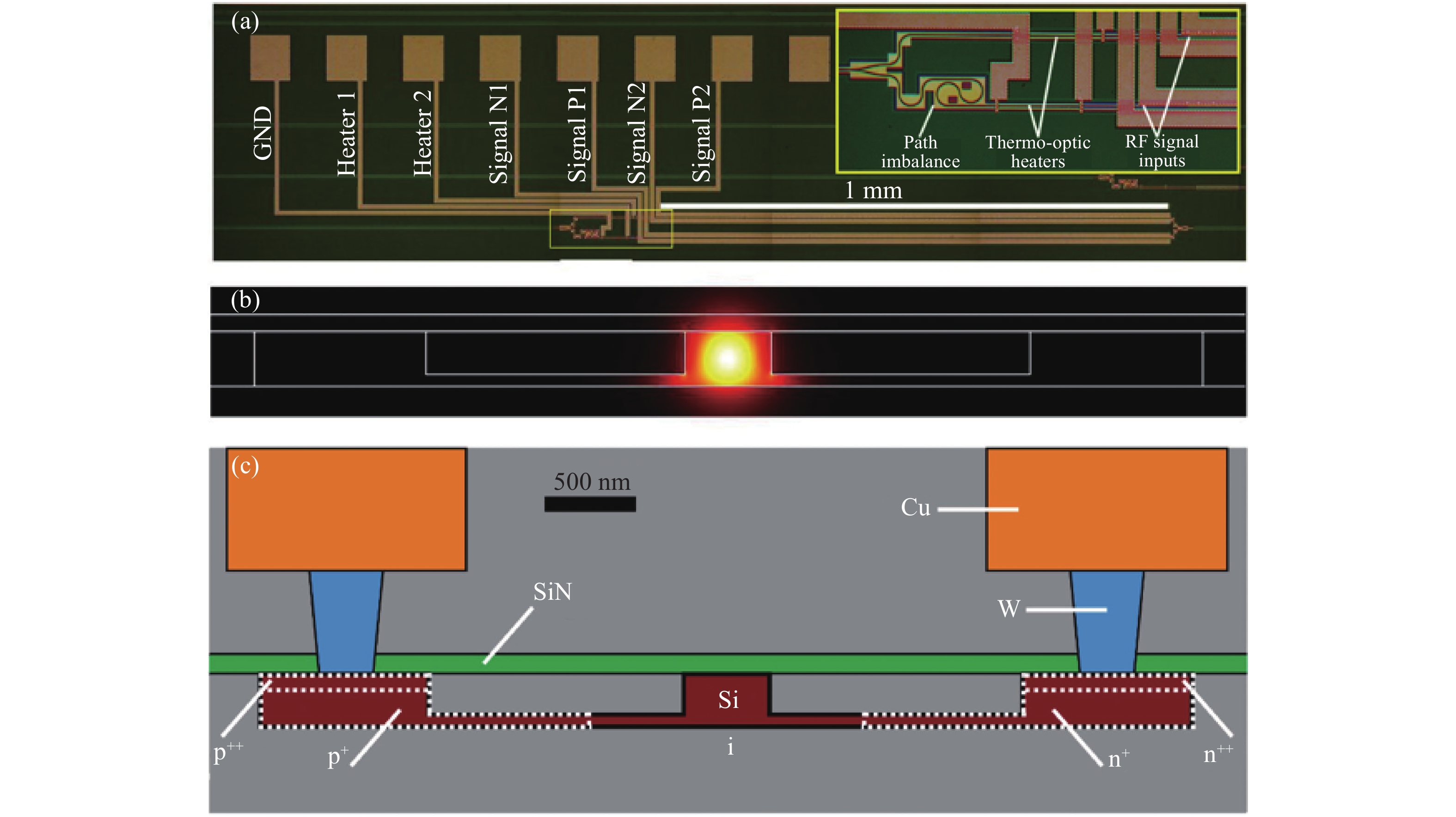
基于载流子浓度变化对半导体材料折射率和吸收系数影响,可以将器件分为两大类,一是改变材料的有效折射率,利用马赫曾德干涉仪将相位调制转变为强度调制的马赫曾德型调制器(MZM);二是直接改变材料的吸收系数,制备强度调制器的光衰减器(VOA)。对于MZM型器件,非对称的两臂会影响器件消光比,因此可以通过引入额外的热调结构调节器件工作点。van Camp M A等人[21]在2012年提出的第一个硅基中红外MZI结构就采用该方法(图2)。该调制器采用了非对称的MZI结构,臂长差85 μm,耦合进波导中的光利用50/50 Y分支结构进入非对称的两臂,通过横向PIN结构在正向偏压下实现光调制效果。该器件采用了独立的热光相移器实现对MZI结构偏置点的控制,见图2。得到的器件工作在2165 nm处,静态消光比约23 dB, Vπ∙L为0.12 V∙mm,采用预加重方法可以得到3 Gbps的眼图信号,以及0.4 GHz的带宽。该工作证明了应用于近红外波段硅基调制器的设计和制备方法同样可以应用在中红外波段,通过进一步设计器件光学和电学结构可以提高器件响应速度和信号传输量。

图 2 (a)制备的MZI调制器的光学显微镜图像,插图中显示了Y分支结构,非对称两臂,热光相移器和高频信号输入端;(b) 波长2165 nm处波导TE模式分布图;(c) PIN 结处的波导的截面图[21]
Figure 2. (a) Optical microscope image of the fabricated MZI modulator. Inset: Magnified detail of the 50/50 Y-junction, differential optical path imbalance, thermo-optic heaters, and RF signal input end; (b) Simulated intensity profile of the fundamental quasi-TE mode at λ = 2165 nm; (c) Cross-section schematic of the PIN diode waveguide active region[21]
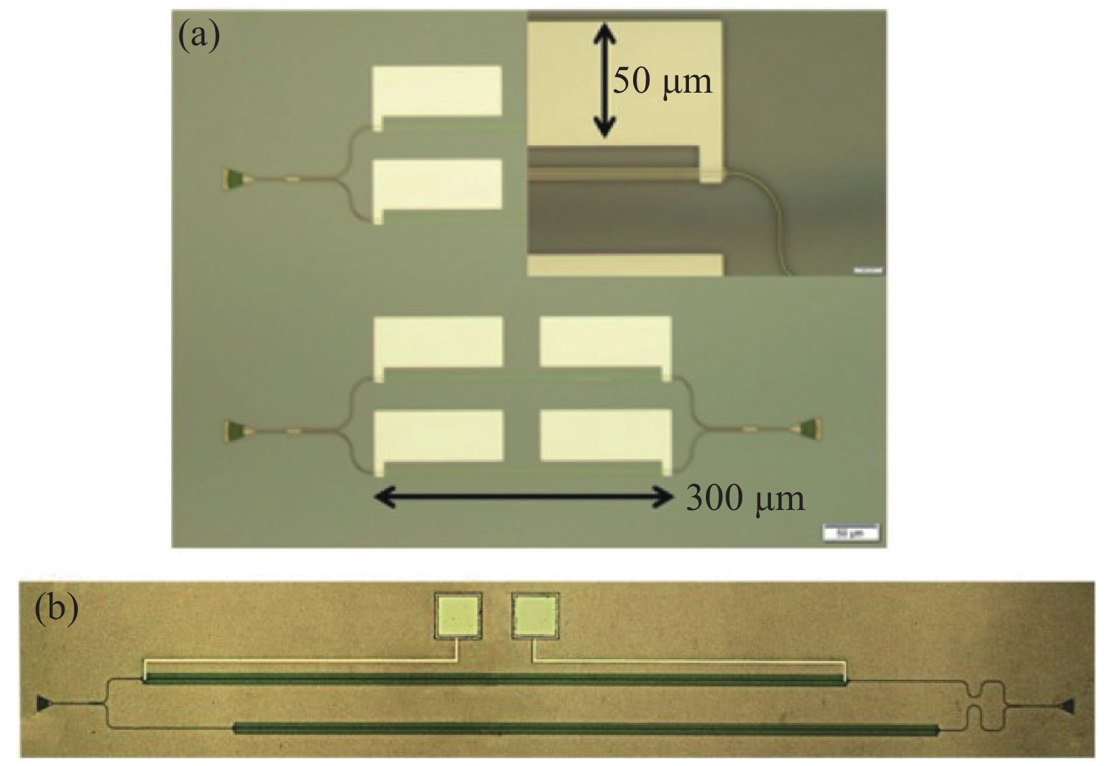
但是由于载流子色散效应对折射率的调制效果小于吸收系数的调制效果,因此MZM型器件很难实现高的消光比。相比于MZM结构,直接强度调制的光衰减器器件结构更加简单,并且可以实现较高的消光比。Nedeljkovic M等人[22]提出了基于SOI平台的直接强度调制的光衰减器(见图3(a)),相比于同时制备的马赫曾德型调制器(见图3(b)),前者在波长3.8 μm处的消光比为34 dB,而后者仅为22.2 dB。为了能够进一步证实Nedeljkovic等人[20]提出的硅的载流子色散效应会随着波长的增加而增大的理论,2014年Thomson D J 等人[23]设计了相关实验。该实验比较了同一个器件在一系列光源波长下的消光比,如图3(a)所示,结果显示:在相同注入电流下长波处的消光更大,证明了在长波长处硅的自由载流子色散效应更强。
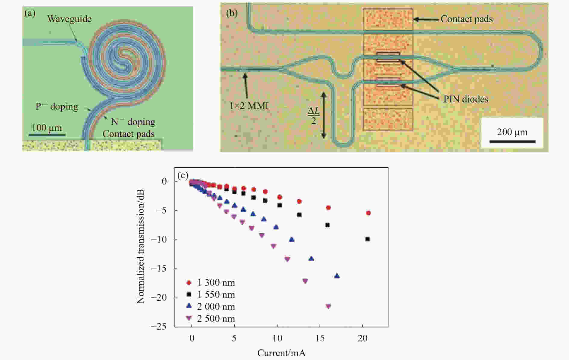
图 3 (a) SOI PIN结的截面图[22];(b) 强度调制的光衰减器显微镜图像,其中红色区域是P型重掺杂,蓝色区域是N型重掺杂[22];(c) 分别在1.31 μm, 1.55 μm, 2 μm和2.5 μm下归一化透射量随注入电流的关系曲线[23]
Figure 3. (a) Schematic cross section of the SOI PIN junction[22]; (b) Optical microscope image of the spiral-shaped PIN electroabsorption modulator. P++ doped areas have been artificially colored in red, and N++ doped areas have been colored in blue[22]; (c) Normalized transmission versus drive current at 1.31 µm, 1.55 µm, 2 µm and 2.5 µm[23]
-
图1表明在中红外波段锗的自由载流子效应高于硅材料,并且锗的透射波长一直延伸到13 μm,因此锗是一个理想的中红外材料。Kang J等人[24]首先在2016年研制出基于绝缘体上锗(Ge-on-insulator, GeOI)平台的锗电光调制器,器件工作在2 μm附近。与硅的载流子注入型器件相似,锗调制器同样采用横向PIN结构。他们仿真计算了2 μm处硅和锗的理论调制效率,并且详细介绍了通过键合和智能剥离方法制备GeOI材料的过程(见图4(a)),透射电子显微镜(TEM)显示得到的GeOI材料质量优良(见图4(b))。制备的器件有源区长度250 μm,从图4(d)可以明显看到随着注入电流的增加波导损耗也逐渐增大,显示了良好的器件调制效果,证明锗材料在中红外光调制方面有很大的潜力。
图 4 (a) GeOI平台的制备过程;(b) GeOI平台的截面TEM图像;(c) GeOI电光调制器的扫描电镜图像;(d) 锗波导损耗随注入电流的变化曲线[24]
Figure 4. (a) Process flow of Ge-on-insulator wafer fabrication; (b) TEM cross-sectional image of the fabricated Ge-on-insulator wafer; (c) Scanning electron microscope image of a GeOI modulator and (d) attenuation characteristics of the Ge variable optical attenuator in the 2 μm band as a function[24]
由于SiO2在2.6~2.9 μm以及3.6 μm以上具有较高的吸收率,因此GeOI在长波波段不再适用。目前利用分子束外延(MBE)技术和化学气相沉积(CVD)技术可以在硅材料上外延出高质量、低位错密度的锗材料,因此硅上锗(Ge-on-Si, GOS)平台将是长波红外波段更佳的选择。2017年,Li T等人[25]提出了基于Ge-on-Si平台的锗电吸收调制器(EAM),这是第一个工作在3.8 μm的直接强度调制器,如图5(a)、(b)所示。随着波长的增加,光场模式尺寸也增加,因此为了控制器件插损大的波导尺寸是不可以避免的,这就造成了较低的调制效率,实验测得该器件需要在7 V的正向偏压下才能实现35 dB的消光比。2019年,Li T等人[16]在此工作的基础上制备了3.8 μm处的MZI型调制器,并且进一步将EAM器件工作波长扩展到了8 μm。拥有1 mm长调制区域的MZI调制器的消光比为13 dB,3.5 V下的Vπ∙L为0.47 V∙cm。脉冲模式信号通过GSG接触电极施加在器件上,可以得到60 MHz的OOK眼图信号。器件在8 μm处的光调制通过红外相机捕捉辐射光线得到,如图5(c)、(d)所示。通过分析吸收效率与PN结电流的关系可以得到8 μm处锗的载流子色散效应是3.8 μm处的4.9倍(8 μm:16.8 dB/A,3.8 μm:3.43 dB/A),同时也证明了随着波长的增加,锗材料的载流子色散效应也相应增强。
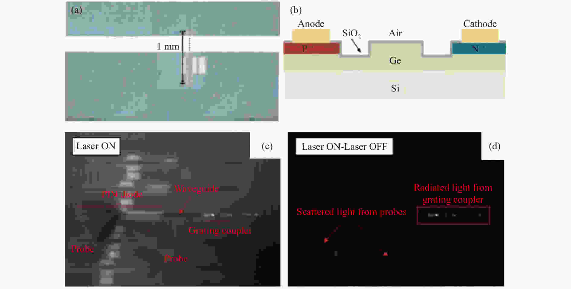
图 5 (a)器件的光学显微镜图像;(b)PIN结截面示意图[25]。用红外相机捕捉从波长为8 μm的量子级联激光器出来的光功率 (c) 发射激光; (d)用“激光器打开”时捕捉到的画面中减去“激光器关闭”时的画面。白色区域的红外光强度高,黑色区域的红外光强度低[16]
Figure 5. (a) Optical microscope image of the device; (b) Cross-section diagram of the PIN junction[25]. Captured LWIR camera image with the QCL tuned to λ=8 μm; (c) When the laser is emitting; (d) When the “laser off” frame is subtracted from the “laser on” frame. White areas show high infrared light intensity, and dark areas show low intensity[16]
载流子注入型调制器多是采用横向PIN结构,在波导两侧进行高掺杂,使得在正向偏压下实现载流子注入。载流子注入型调制器工艺简单、对制备工艺要求低、器件插损小,相比于载流子耗尽型调制器可以实现更大的消光比,但是载流子注入型调制器的电学响应速度较低,通常小于1 GHz,这使得其在需要相对较高速度的光通信中的应用受到限制。提高器件频率响应带宽的一种方式是降低少数载流子寿命,可以通过对本征波导内进行掺杂复合中心来实现,但是无疑增大了工艺难度和器件损耗。尽管如此,针对速度要求不高的片上传感等领域,载流子注入型调制器具有较好的应用潜力。
-
对于长波光通信系统来说,高速中红外调制器是必不可少的一个环节,也是目前中红外通信面临的一个挑战,因此有诸多研究人员在高速调制方面做出了努力。对于硅基载流子耗尽型光电调制器,它利用载流子在反向电场作用下的高速漂移运动,而且有较高的掺杂使得少子寿命缩短,因此最有望实现高速调制器。但是如何解决载流子耗尽型调制器消光比和调制效率较低问题是关键之处。对于波导型结构来说,波导模式光场和PN结电场之间的重叠积分越大,器件消光比和调制效率也会更大,这就要求合适的离子注入掺杂位置。
2018年,Cao W等人[26]仿真分析了高掺杂区距离波导的位置和PN结的位置对带宽和损耗的影响,设计了非对称掺杂结构的马赫曾德型调制器,如图6所示。这也是第一个实验制备的2 μm高速硅电光调制器。实验结果表明,MZM在−4 V的反向偏压下调制效率为2.68 V∙cm,在2 μm波长处可以实现20 Gbit/s的数据调制。对于高速硅基调制器来说,微环也是常用的调制器结构。该文章同时设计并制备了2 μm处的微环调制器(MRR),如图6(b)所示,微环的弯曲半径为10 μm。为了提高器件的消光比,他们使其工作在正反偏混合模式下,将直流偏置点设定为正向的0.5 V,Vpp为2 V,调制速率为3 Gbit/s,动态消光比2.3 dB。相较于之前Cao W等人的工作,Hagan D E等人[27]优化了微环有源区的掺杂结构,设计了更大消光比和带宽的全通MRR。实验得到的消光比20 dB,由于受到2 μm商用探测器的限制,测得的最大带宽12.5 GHz。
对于光通信系统来说,仅仅20 Gbit/s的数据传输量是远远不够的,这需要提升器件的带宽,而对于马赫曾德型调制器来说,其带宽与器件自身RC常数和行波电极密不可分,因此,如何缩小器件电容,做到电路和光路匹配至关重要。 Li W等人[28]通过采用GS电极形成推挽结构,配合60 Ω的终端匹配电阻实现了50 Gbit/s的高速硅调制器(误码率低于3.8×10−3),如图7(a)所示。该团队在此基础上设计了反向串联PN结结构,利用该结构使得器件电容减半,并且同样采用单端推挽结构,高频信号通过GS接触电极以及T型传输线施加在器件上,实现电信号和光信号的匹配,器件结构如图7(b)、(c)所示。该器件在中红外波段第一次获得了80 Gbit/s的PAM-4信号,器件最大带宽为18 GHz。由于载流子耗尽型调制器需要在波导上进行N和P区的浅注入,因此对工艺水平要求高,但目前锗材料的工艺条件还未开发完全,因此还未有锗的载流子耗尽型器件被报道。表1总结了中红外硅基电光调制器的类型和性能。

表 1 中红外硅基电光调制器的类型及性能
Table 1. Types and performance of mid-infrared silicon-based electro-optic modulators
Ref. Platform Operating wavelength/μm Type Extinction ratio Vπ∙L/V∙mm Data rate/Bandwidth Years Carrier-injection [20] SOI 2.165 MZM 23 dB 0.12 3 Gbps/0.4 GHz 2012 [21] SOI 3.8 EAM 34 dB - 60 Mbit/s 2014 MZM 22.2 dB 0.052 125 Mbit/s [24] GOS 3.8 EAM 35 dB - 6 MHz 2017 [15] GOS 3.8 MZM 13 dB 0.47 60 MHz 2019 8 EAM 16.8 dB/A - - Carrier-depletion [25] SOI 2 MZM - 2.68 20 Gbit/s 2018 MRR 15 dB - 3 Gbit/s [26] SOI 2 MRR 20 dB 2.6 V∙cm 12.5 GHz 2020 [27] SOI 2 MZM 20 dB 1 50 Gbit/s 2020 [28] SOI 2 MZM 22 dB 1.6 80 Gbit/s(PAM-4)/18 GHz 2021 载流子耗尽型调制器是目前光通信中的主流器件,可以实现较快的调制速度。载流子耗尽型调制器多采用马赫曾德型结构,器件尺寸较大,并且由于对波导进行了掺杂带来了额外的光吸收损耗。与载流子注入型的调制器相比,其调制效率较低,器件消光比也较低。进一步提高载流子耗尽型器件的带宽和调制效率是研究的方向之一。但是,目前在中红外波段主要还是基于SOI衬底,限制了更长波长的器件的使用。开发和优化硅基或SOI基的锗波导和器件工艺是提高其工作波长的主要途径。此外,高速中红外调制器的在光通信中的应用场景还不明确,需要研究人员和行业的进一步探索和发展。
-
除电光调制外,热光调制也是硅、锗调制器的主要调制机理。热光调制主要利用材料的折射率会受温度影响的原理,通过改变器件温度,进而改变折射率来调节光的损耗和相位,从而实现对光的调制。Frey B等人[18]首先通过实验得到了硅、锗在中红外波段的热光系数。Nedeljkovic M等人[15]第一次研制了2 μm以上波长处的硅基热光调制器,并且提出了利用调制器代替斩波器和锁相放大器的组合提高传感系统信噪比的概念。
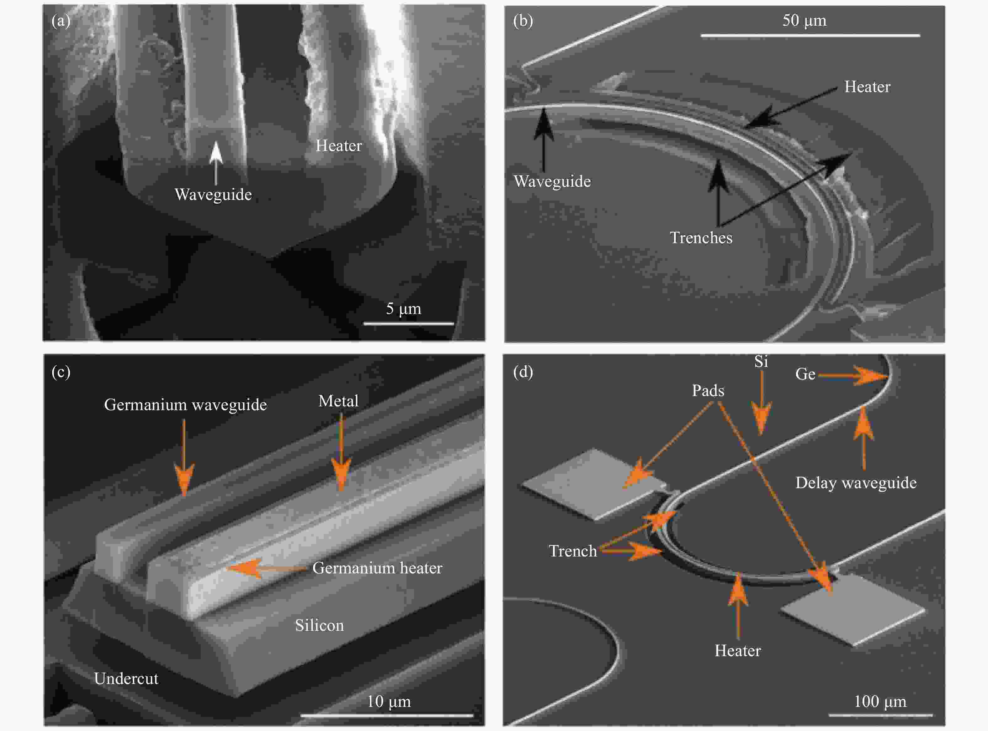
对于热光调制器来说,功耗是非常重要的参数,可以通过采用高电阻率热极材料,缩小热极材料与波导间距、增加调制区长度等方法降低功耗。而对于Ge-on-Si和Ge-on-SOI平台来说,硅材料高的热导率也是影响其功耗的主要原因。Malik A等人[30]利用实验证明并解决了这一问题。他们制备了工作波长为5 μm的Ge-on-Si和Ge-on-SOI热光调制器,如图8所示,热极材料采用Ti/Au合金。实验结果显示:Ge-on-Si热光相移器的调制效率很低,对于700 μm长的热光调制器件,实现2π的相移需要700 mW的功率。这是因为衬底硅材料导热性能好,热导率高达130 W/(m·K),导致其类似于一个散热器,加热电极对锗波导加热的热量会很快通过硅衬底传导出去,大大提高了器件的功耗。为了降低功耗,他们采用了聚焦离子束(FIB)技术移除热调区域下方的硅材料,形成空气绝热层来对波导“保温”。实验得到移除有源区下方硅之后,210 μm长的器件实现2π的相移仅需要80 mW功率。除此之外,作者采用相同的设计原理和制备方式得到了基于Ge-on-SOI平台的相移器,并对比了移除有源区锗下方的硅前后器件实现2π相移所需的功率,发现移除硅之后器件的调制功率降低了80%,对210 μm长的器件仅需要20 mW。
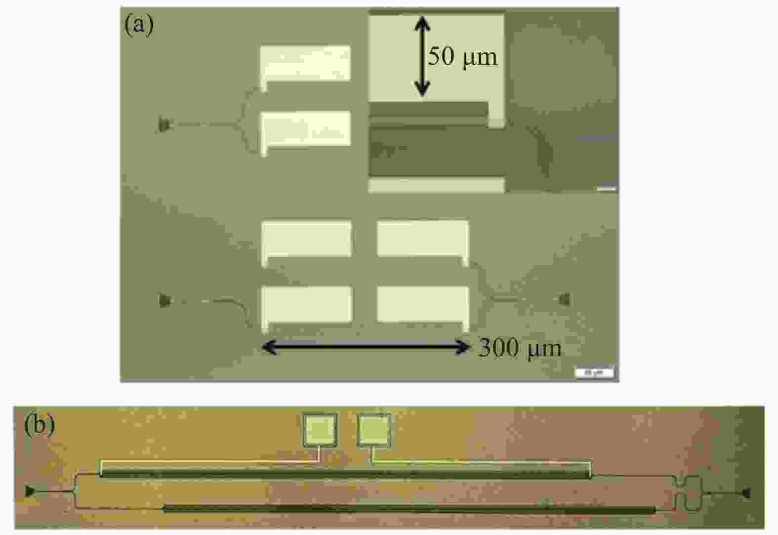
SiO2的热导率远小于硅材料,因此可以利用GeOI或者SOI材料制备热光调制;器,从而省略聚焦离子束(FIB)工艺步骤,简化制备流程。 Fujigaki X等人[31]提出了一种基于GeOI平台的高效率锗热光调制器,如图9(a)所示,该器件工作在1.95 μm下,加热电极采用Pt材料。实验证明:对于GeOI平台来说,实现π的相移仅需要7.8 mW,这也是目前锗的热光调制器取得的最好结果。为了更好与CMOS工艺兼容,Yu T等人[32]在2019年提出了工作在2 μm处的硅热光调制器,如图9(b)所示,热极材料采用长度1500 μm的TiN材料。利用传输谱和任意波形发生器对器件的消光比和信号传输速度进行了测试,得到消光比为27 dB,对于20 kHz的驱动信号, 上升时间和下降时间约为6 μs和4 μs。
热光调制器利用波导材料的热光效应,对热极材料通电产生焦耳热传导给波导,从而实现器件的相位及强度的调节。由于热产生和热传导是非常慢的响应过程,因此热光调制器的响应速度非常低,主要应用到传感系统等不需要快速通信的场景中。热光相移器的消光比和功耗是主要关心的问题,需要进一步地创新改进。
-
中红外波段有着独特的特征使得其在传感、生物分子检测、安全等领域都有广泛的应用前景。更重要的是它拥有3~5 μm、8~12 μm两个大气窗口,可以用来解决随着5G时代到来而带来的数据量传输量急剧增大的问题,与近红外波段相比,中红外的信息安全性更高。高速、低损、低功耗的调制器是光通信和片上传感系统中至关重要的一部分,在中红外波段硅和锗材料的自由载流子等离子色散效应更强,因此,发展中红外硅基调制器具有可行性和良好的应用前景。基于以上动机,笔者分别总结了主流的几种硅基中红外调制器(载流子注入型调制器、载流子耗尽型调制器、热光调制器)的器件特点和发展现状。目前,硅基中红外调制器的发展距离实用化仍有较长的距离,特别是锗基材料的相关工艺尚不成熟,使得高性能的中红外调制器大多采用纯硅的SOI衬底,难以进一步扩展使用波长。因此,高性能的中红外调制器的发展不仅需要器件结构上的创新,还需要对锗基材料的标准化工艺进行深入的研究。此外,随着中红外分立器件的研制成功,相信中红外硅基光电子片上集成芯片和系统在不久的将来也会相继面世。
Research progress of mid-infrared silicon-based modulators (Invited)
-
摘要: 硅材料在1.1~8.5 μm有非常低的吸收损耗,因此硅基光电子学有望扩展到中红外波段。并且随着通信窗口扩展、气体分子检测、红外成像等应用需求的出现,硅基中红外波段器件研发工作的开展势在必行。在中红外波段硅基光电子器件中,硅基调制器有着举足轻重的地位:它是长波光通信链路中不可或缺的一环,还可以应用在片上传感系统中提高信噪比、实现光开关等功能。研究发现,相比于近红外波段,硅和锗材料在中红外波段有更强的自由载流子效应和热光效应,因此,基于硅基材料的中红外调制器具有独天得厚的优势。系统总结了中红外硅基调制器的发展趋势和研究现状,介绍了基于硅和锗材料的电光调制器以及热光调制器的工作原理和最新研究进展,最后对中红外硅基调制器进行了总结与展望。Abstract: Silicon-based photonics is expected to be extended to the mid-infrared (MIR) wavelength, due to the low absorption of silicon (Si) material in the range of 1.1 μm to 8.5 μm. With the needs emergence of communication window expansion, gas molecular detection, infrared imaging and other applications, the development of silicon-based devices in the mid-infrared wavelength is imperative. Silicon-based modulator plays an important role in the research and development of silicon-based optoelectronic devices in MIR. It is an indispensable link in long wave optical communication system, and can be used in on-chip sensing system to improve the signal-to-noise ratio and realize optical switching. It is found that silicon and germanium materials have greater free carrier effect and thermal-optical effect in the MIR band than that in the near-infrared band (NIR). It is proved that silicon-based materials have unique advantages in the development of mid-infrared modulators. The development trend and research status of MIR silicon-based modulators were summarized. The working principle and latest research progress of electro-optic modulators and thermal-optic modulators based on silicon and germanium materials were introduced. Finally, the mid-infrared silicon-based modulators were summarized and prospected.
-
Key words:
- mid-infrared /
- silicon-based optoelectronics /
- modulator
-

图 2 (a)制备的MZI调制器的光学显微镜图像,插图中显示了Y分支结构,非对称两臂,热光相移器和高频信号输入端;(b) 波长2165 nm处波导TE模式分布图;(c) PIN 结处的波导的截面图[21]
Figure 2. (a) Optical microscope image of the fabricated MZI modulator. Inset: Magnified detail of the 50/50 Y-junction, differential optical path imbalance, thermo-optic heaters, and RF signal input end; (b) Simulated intensity profile of the fundamental quasi-TE mode at λ = 2165 nm; (c) Cross-section schematic of the PIN diode waveguide active region[21]
图 3 (a) SOI PIN结的截面图[22];(b) 强度调制的光衰减器显微镜图像,其中红色区域是P型重掺杂,蓝色区域是N型重掺杂[22];(c) 分别在1.31 μm, 1.55 μm, 2 μm和2.5 μm下归一化透射量随注入电流的关系曲线[23]
Figure 3. (a) Schematic cross section of the SOI PIN junction[22]; (b) Optical microscope image of the spiral-shaped PIN electroabsorption modulator. P++ doped areas have been artificially colored in red, and N++ doped areas have been colored in blue[22]; (c) Normalized transmission versus drive current at 1.31 µm, 1.55 µm, 2 µm and 2.5 µm[23]
图 4 (a) GeOI平台的制备过程;(b) GeOI平台的截面TEM图像;(c) GeOI电光调制器的扫描电镜图像;(d) 锗波导损耗随注入电流的变化曲线[24]
Figure 4. (a) Process flow of Ge-on-insulator wafer fabrication; (b) TEM cross-sectional image of the fabricated Ge-on-insulator wafer; (c) Scanning electron microscope image of a GeOI modulator and (d) attenuation characteristics of the Ge variable optical attenuator in the 2 μm band as a function[24]
图 5 (a)器件的光学显微镜图像;(b)PIN结截面示意图[25]。用红外相机捕捉从波长为8 μm的量子级联激光器出来的光功率 (c) 发射激光; (d)用“激光器打开”时捕捉到的画面中减去“激光器关闭”时的画面。白色区域的红外光强度高,黑色区域的红外光强度低[16]
Figure 5. (a) Optical microscope image of the device; (b) Cross-section diagram of the PIN junction[25]. Captured LWIR camera image with the QCL tuned to λ=8 μm; (c) When the laser is emitting; (d) When the “laser off” frame is subtracted from the “laser on” frame. White areas show high infrared light intensity, and dark areas show low intensity[16]
表 1 中红外硅基电光调制器的类型及性能
Table 1. Types and performance of mid-infrared silicon-based electro-optic modulators
Ref. Platform Operating wavelength/μm Type Extinction ratio Vπ∙L/V∙mm Data rate/Bandwidth Years Carrier-injection [20] SOI 2.165 MZM 23 dB 0.12 3 Gbps/0.4 GHz 2012 [21] SOI 3.8 EAM 34 dB - 60 Mbit/s 2014 MZM 22.2 dB 0.052 125 Mbit/s [24] GOS 3.8 EAM 35 dB - 6 MHz 2017 [15] GOS 3.8 MZM 13 dB 0.47 60 MHz 2019 8 EAM 16.8 dB/A - - Carrier-depletion [25] SOI 2 MZM - 2.68 20 Gbit/s 2018 MRR 15 dB - 3 Gbit/s [26] SOI 2 MRR 20 dB 2.6 V∙cm 12.5 GHz 2020 [27] SOI 2 MZM 20 dB 1 50 Gbit/s 2020 [28] SOI 2 MZM 22 dB 1.6 80 Gbit/s(PAM-4)/18 GHz 2021  下载: 导出CSV
-
[1] Chen H D, Zhang Z, Huang B J, et al. Progress in complementary metal-oxide-semiconductor silicon photonics and optoelectronic integrated circuits [J]. Journal of Semiconductors, 2015, 36: 121001-121013. doi: 10.1088/1674-4926/36/12/121001 [2] Milošević M M, Nedeljkovic M, Ben Masaud T M, et al. Silicon waveguides and devices for the mid-infrared [J]. Applied Physics Letters, 2015, 101: 121105. [3] Nedeljkovic M, Khokhar A Z, Hu Y, et al. Silicon photonic devices and platforms for the mid-infrared [J]. Optical Materials Express, 2013, 3: 1205-1214. doi: 10.1364/OME.3.001205 [4] Hu T, Dong B, Luo X, et al. Silicon photonic platforms for mid-infrared applications [Invited] [J]. Photonics Research, 2017, 5: 417-430. doi: 10.1364/PRJ.5.000417 [5] Gallacher K, Millar R W, Griškevičiūtė U, et al. Components for integrated Ge on Si for mid-infrared photonic sensors [C]//2018 IEEE Photonics Society Summer Topical Meeting Series (SUM), 2018: 177-178. [6] Chakravarty S, Yan H, Zou Y, et al. Mid-infrared silicon photonic devices and sensors [C]//2017 IEEE Photonics Society Summer Topical Meeting Series (SUM), 2017: 183-184. [7] Shankar R, Lončar M. Silicon photonic devices for mid-infrared applications [J]. Nanophotonics, 2017, 3: 329-341. [8] Zou Y, Chakravarty S, Chung C J, et al. Mid-infrared silicon photonic waveguides and devices [Invited] [J]. Photonics Research, 2018, 6: 254-276. doi: 10.1364/PRJ.6.000254 [9] Alonso-Ramos C, Nedeljkovic M, Benedikovic D, et al. Germanium-on-Silicon mid-infrared grating couplers with low-reflectivity inverse taper excitation [J]. Opt Lett, 2016, 41: 4324-4327. doi: 10.1364/OL.41.004324 [10] Radosavljevic S, Kuyken B, Roelkens G. Efficient 5.2 microm wavelength fiber-to-chip grating couplers for the Ge-on-Si and Ge-on-SOI mid-infrared waveguide platform [J]. Opt Express, 2017, 25: 19034-19042. doi: 10.1364/OE.25.019034 [11] Nedeljkovic M, Penades J S, Mitchell C J, et al. Surface-grating-coupled low-loss Ge-on-Si rib waveguides and multimode interferometers [J]. IEEE Photonics Technology Letters, 2015, 27: 1040-1043. doi: 10.1109/LPT.2015.2405611 [12] Rouifed M, Littlejohns C G, Tina G X, et al. Low loss SOI waveguides and MMIs at the MIR wavelength of 2 μm [J]. IEEE Photonics Technology Letters, 2016, 28: 2827-2829. doi: 10.1109/LPT.2016.2623319 [13] Liu Y, Li Z, Li D, et al. Thermo-optic tunable silicon arrayed waveguide grating at 2 μm wavelength band [J]. IEEE Photonics Journal, 2020, 12: 1-8. [14] Li X, Peng L, Liu Z, et al. 30 GHz GeSn photodetector on SOI substrate for 2 µm wavelength application [J]. Photonics Research, 2021, 9(4): 494-500. doi: 10.1364/PRJ.413453 [15] Nedeljkovic M, Stankovic S, Mitchell C J, et al. Mid-infrared thermo-optic modulators in SOI [J]. IEEE Photonics Technology Letters, 2014, 26: 1352-1355. [16] Li T T, Nedeljkovic M, Hattasan N, et al. Ge-on-Si modulators operating at mid-infrared wavelengths up to 8 μm [J]. Photonics Research, 2019, 7: 828-836. [17] Soref R, Bennett B. Electrooptical effects in silicon [J]. IEEE Journal of Quantum Electronics, 1987, 23: 123-129. [18] Atad-Ettedgui E, Frey B J, Antebi J, et al. Temperature-dependent refractive index of silicon and germanium [J]. Optomechanical Technologies for Astronomy, 2006, 6273: 62732J. [19] Mashanovich G, Cao W, Qu Z, et al. Mid-infrared silicon photonics for communications [J]. International Journal of Electrical Engineering and Computing, 2019, 3: 32-36. [20] Nedeljkovic M, Soref R, Mashanovich G Z. Predictions of free-carrier electroabsorption and electrorefraction in Germanium [J]. IEEE Photonics Journal, 2015, 7: 1-14. [21] Van Camp M A, Assefa S, Gill D M, et al. Demonstration of electrooptic modulation at 2165 nm using a silicon Mach-Zehnder interferometer [J]. Opt Express, 2012, 20: 28009-28016. doi: 10.1364/OE.20.028009 [22] Nedeljkovic M, Littlejohns C G, Khokhar A Z, et al. Silicon-on-insulator free-carrier injection modulators for the mid-infrared [J]. Opt Lett, 2019, 44: 915-918. doi: 10.1364/OL.44.000915 [23] Thomson D J, Shen L, Ackert J J, et al. Optical detection and modulation at 2 microm-2.5 microm in silicon [J]. Opt Express, 2014, 22: 10825-10830. doi: 10.1364/OE.22.010825 [24] Kang J, Takenaka M, Takagi S. Novel Ge waveguide platform on Ge-on-insulator wafer for mid-infrared photonic integrated circuits [J]. Opt Express, 2016, 24: 11855-11864. [25] Li T T, Nedeljkovic M, Hattasan N, et al. Mid-infrared Ge-on-Si electro-absorption modulator [C]//2017 IEEE 14th International Conference on Group IV Photonics (GFP), 2017: 7-8. [26] Cao W, Hagan D, Thomson D J, et al. High-speed silicon modulators for the 2 μm wavelength band [J]. Optica, 2018, 5: 1055. doi: 10.1364/OPTICA.5.001055 [27] Hagan D E, Ye M, Wang P, et al. High-speed performance of a TDFA-band micro-ring resonator modulator and detector [J]. Opt Express, 2020, 28: 16845. doi: 10.1364/OE.393538 [28] Li W, Li M, Zhang H, et al. 50 Gbit/S silicon modulator operated at 1950 nm [C]//2020 Optical Fiber Communications Conference and Exhibition (OFC), 2020: 1-3. [29] Wang X, Shen W, Li W, et al. High-speed silicon photonic Mach-Zehnder modulator at 2-µm [J]. Photonics Research, 2021, 9: 535-540. doi: 10.1364/PRJ.417107 [30] Malik A, Dwivedi S, Landschoot L V, et al. Ge-on-Si and Ge-on-SOI thermo-optic phase shifters for the mid-infrared [J]. Opt Express, 2014, 22: 28479-28488. doi: 10.1364/OE.22.028479 [31] Fujigaki T, Takagi S, Takenaka M. High-efficiency Ge thermo-optic phase shifter on Ge-on-insulator platform [J]. Opt Express, 2019, 27: 6451-6458. [32] Yu T, Liu Y, Li Z, et al. Integrated thermo-optic switch for 2 µm spectral band[C]//International Photonics and Opto-Electronics Meeting, 2019: OTu2B.4. -

 点击查看大图

计量
- 文章访问数: 390
- HTML全文浏览量: 128
- PDF下载量: 110
- 被引次数: 0

