


-
近年来,具有单光子检测能力的单光子雪崩二极管(Single Photon Avalanche Diode, SPAD)以其灵敏度高、响应速度快、抗干扰能力强、体积小等优点,在诸如激光雷达[1-3]、量子通信[4]、荧光光谱分析[5]等弱光探测领域得到了广泛应用。SPAD探测器作为一种新型非线性器件,制作工艺复杂。而且SPAD阵列的各类应用需要检测传感信号的读出电路(Readout Integrated Circuit, ROIC)与之配套,以实现SPAD探测器雪崩信号的提取和处理。各类应用对阵列规模、探测器信号的提取和处理能力的要求也越来越高。同时大规模阵列导致的寄生效应、功耗、面积等问题越来越突出,严重影响成像质量,阵列型SPAD读出电路的设计面临很大的挑战[6-7]。而如果要与高性能SPAD阵列匹配,读出电路就必须具备高速、高精度、低功耗的性能特点。因此,单光子红外探测技术的发展既依赖于先进传感器的研制,又离不开具备雪崩信号检测与处理能力的专用集成电路的研发。
作为成像系统中的核心单元,ROIC需要为SPAD提供最佳偏置的工作条件,并提取雪崩信号,随后对雪崩信号进行高精度、高速实时处理和数据传输。其中,对探测器雪崩信号进行检测的电路被称为接口电路,接口电路为SPAD传感器提供最佳的偏置条件,并完成雪崩信号的检测和雪崩淬灭,最后输出标准数字信号供后续电路处理。后续电路会根据系统具体成像应用的需求,对雪崩信号执行数字量化、计算等操作,最终转换、输出为遵循一定格式要求的数据。下文分别对接口电路与信号处理电路的关键技术进行分析。
-
SPAD正常工作时主要有待测、雪崩、截止三种状态。处于雪崩状态时,SPAD会产生能够自维持的雪崩电流,需要采用相应的电流抑制措施使得雪崩过程及时停止,否则器件将造成不可逆的损坏[8]。因此,雪崩淬灭电路被提出用来解决上述问题[9]。淬灭电路属于动态偏置电路,能够通过切换反偏电压来控制SPAD的工作状态和工作模式,即雪崩倍增效应发生之后,SPAD两端电压会降低使得SPAD快速恢复到初始状态,为探测下一个光子做准备。
根据反偏电压受控方式的不同,淬灭方式主要分为被动淬灭、主动淬灭以及主、被动混和淬灭三类,三种方式在电路复杂程度、淬灭和复位时间、检测准确率等方面各有优劣。
被动淬灭电路的结构示意图如图1(a)所示,主要通过与SPAD串联的大电阻实现淬灭功能,此方式结构简单,但是感应电阻会产生较大的面积消耗[10],且感应电阻与寄生电容共同形成的RC时间常数较大,会导致SPAD的恢复时间较长。该方式一般应用于单个探测器或对检测速度要求不高的场景。

图 1 (a)被动淬灭电路; (b)主动淬灭电路
Figure 1. (a) Passive quenching circuit; (b) Active quenching circuit
主动淬灭电路的结构示意图如图1(b)所示,在被动淬灭电路的基础上增加了反馈回路和控制开关,从而实现雪崩电流的主动淬灭。该方式电路结构较为复杂,但是复位时间明显降低,有效减小了死区时间,提高了最高工作频率[11]。
在SPAD阵列的实际应用中,要求接口电路能快速提取雪崩信号并进行淬灭。但是由于像素电路的面积和功耗有限,所以主动淬灭电路的具体实现有多种方式。可以采用电阻或电容感应雪崩电流,其中电阻或电容的取值大小仍是关键,需要兼顾电路的速度、功耗和面积。其次检测阈值的选取也比较关键,阈值的选取与探测器的暗电流、雪崩电流相关。该参数可以通过电路建模计算与仿真择优选择,从而实现较高的信噪比。
近年来,随着SPAD阵列规模的不断扩大,各研究团队对SPAD接口电路也有了更高的要求和更深入的研究。
为了解决SPAD击穿电压不一致的问题,许多接口电路具备了区域级或像素级调节SPAD反向偏压的功能[12],可以分区域,甚至逐个像素精确调节反向偏压。东南大学提出了一种可用于阵列的反偏电压调节电路[13]。如图2所示,SPAD增益波动抑制电路采用DAC方式提供偏置点电压,位于像素外部,而像素内部则采用主动淬灭方式,工作原理如下:根据每个SPAD探测器的击穿电压,确定每个数据选择器的输入信号。将一连串的预设置的输入信号DIN通过移位寄存器传输给每个数据选择器并锁存,同时将电压调节器各结点输出电压提供给每个选择该电压的像素,进而实现多像素APD的反偏电压可调,调节之后,阵列的暗计数一致性得到明显改善。

图 2 偏压调节电路架构图
Figure 2. An architecture realizing constant excess bias control
在光子计数应用中,探测器工作于自由探测模式,根据探测器特性及应用场景灵活设置死区时间,可以在满足较高探测效率的前提下减少电路的后脉冲及暗计数。2019年,西南技术物理研究所的团队提出了一种钟控死区时间可调架构[14],电路架构如图3所示。该架构引入了时钟信号,在雪崩信号的触发下,驱动判别模块进行时钟周期的计数,当计数码与调节码一致时,触发复位脉冲的产生,因此调节输入时钟的周期即可控制死区时间调节分辨率及最小死区时间。

图 3 钟控死区时间可调架构
Figure 3. Clock controlled dead-zone-time adjustable architecture
此外,一般SPAD使用的电压均为10 V以上,远远高于ROIC的电源电压,为了保护读出电路,需要在电路上加入高压击穿保护电路,但由于ROIC的工艺一般为普通CMOS工艺,耐压能力在5 V以内,而高压管非常占用面积,无法在像素集成,目前有一些研究团队提出了一些电路结构,但在阵列应用中目前尚无较好的解决方案。
SPAD接口电路需要具有雪崩信号提取和淬灭功能,并根据应用需求有像素级SPAD反偏电压调节和死区时间调节、自恢复等额外功能。在紧凑的像素面积条件限制下实现雪崩信号的快速淬灭、提取以及各类功能是当前SPAD接口电路面临的主要问题。
-
典型的基于光子飞行时间(Time of Flight, TOF)的成像系统架构如图4所示。系统工作时,首先由主机/延时器(Host/Delayer)发出系统启动指令,ROIC完成测量前的电路复位,系统处于待测状态。随后主机发出激光发射指令EN,激光器向目标发射激光,同时ROIC中所有像素的时间-数字转换器(Time-to-digital Converter, TDC)开始计时。直到像素的探测器检测到反射的光子,TDC才停止计时。ROIC再将各个像素量化后的数据逐像素传出,实现图像处理与显示。
TDC直接将时间模拟信号转换为数字信号,同样需要具有高精度和高转换速度的性能。而利用时间放大、时间追赶等电路架构,传统独立TDC的时间分辨率已经可以达到1 ps以下[15-16]。但是,由于像素电路受到严格的面积和功耗限制(一般要求像素中心间距在50 μm以下),所以上述高精度TDC中常用的实现方法无法用于阵列TDC,导致阵列型TDC的精度难以提升。
在转换位数有限的条件下,TDC的量化精度和量程相互制约。对于宽动态范围的量化场合,传统的单模式TDC难以协调精度和量程之间的矛盾。而且单模式TDC如需改善分辨率、提高精度,就需要不断减小量化单位,导致时钟频率不断提高、功耗显著增大,因此,量化精度的提高也会受到系统功耗的限制。而由不同类型的单模式TDC共同组合(时空域变换)构成的分段式TDC,即有多种不同最低有效位(Least Significant Bit, LSB)作为量化单位的组合式TDC,能够以更低的代价高效实现多位量化,兼顾量程和精度,同时可以避免时钟频率和系统功耗的过度增加。
光子计时读出电路的主要性能指标为阵列规模、像素面积、时间分辨率、计时量程、帧频。其中时间分辨率是关键指标,阵列时间-数字转换电路受像素面积的严格限制,不能采用复杂电路结构,因此是一个较难实现的技术。同时时间分辨率与计时量程也是一个折中的关系,在像素面积和功耗的严格限制下,需要根据应用需求,选择到底是要看的远,还是要看的更清的问题。表1从工艺、像素规模、像元中心距、时间分辨率、计时量程、帧率和系统功耗对比了当前先进的光子计时读出电路的研究情况。
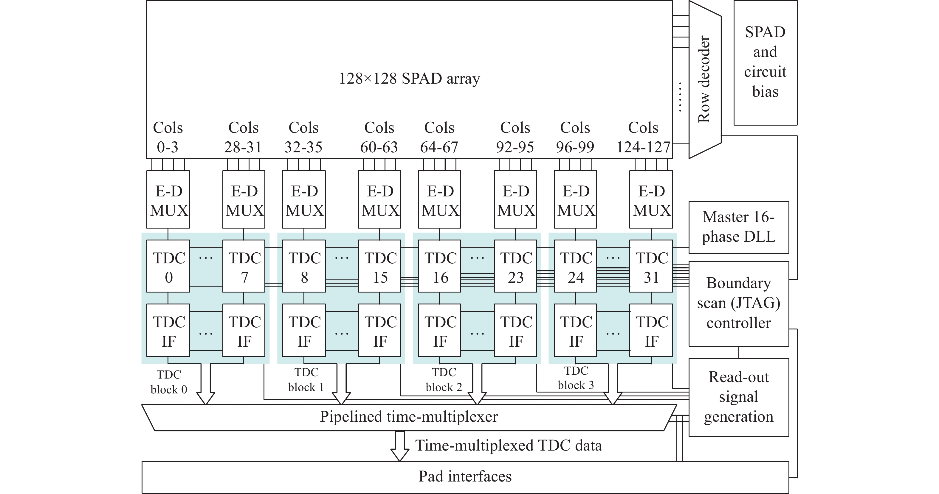
其次随着阵列规模的增大,TDC的功耗成为制约ROIC规模扩大的主要因素。瑞士洛桑理工学院是较早实现大面阵读出电路的研究机构之一[17],2008年,该机构提出了一种基于TDC共享架构的低功耗ROIC,阵列规模扩展至128×128,时间分辨率最高可达97 ps,系统架构如图5所示。在该阵列ROIC中仅有32个TDC模块,采用行扫描机制分时共享TDC,且一行中每四个像素为一组,一组共享一个TDC。由于采用TDC共享机制和逐行扫描方案,所以该系统仅需32个TDC即可实现128×128阵列的量化工作,极大地降低了系统功耗。又因为TDC位于像素阵列外部,面积较为宽裕,所以可以采用一种较为复杂的多段式TDC架构,最终系统的时间分辨率能够达到百皮秒以内。
表 1 光子计时读出电路的性能对比
Table 1. Performance comparison of photon timing readout circuit
Year 2018[18] 2020[19] 2020[20] 2018[21] 2019[22] Institution MIT Lincoln Laboratory University of Edinburgh Swiss Federal Institute of Technology Delft University of Technology Southeast University Technology 0.18 μm CMOS 40 nm CMOS 0.35 μm CMOS 0.18 μm CMOS 0.18 μm CMOS Pixel array 256×128 128×128 32×128 252×144 64×64 Pixel pitch 50 μm 40 μm×20 μm 40 μm 28.5 μm 50 μm TDC resolution 500 ps 100 ps 78 ps 48.8 ps 1000 ps TDC range - 23.3 ns 640 ns 333 ns 4000 ns Frame rate - 500 fps 20 fps 31.25 kfps 20 kfps Power - 185 mW - 2540 mW 490 mW 
图 4 基于SPAD阵列的TOF成像系统
Figure 4. TOF imaging system based on SPAD array
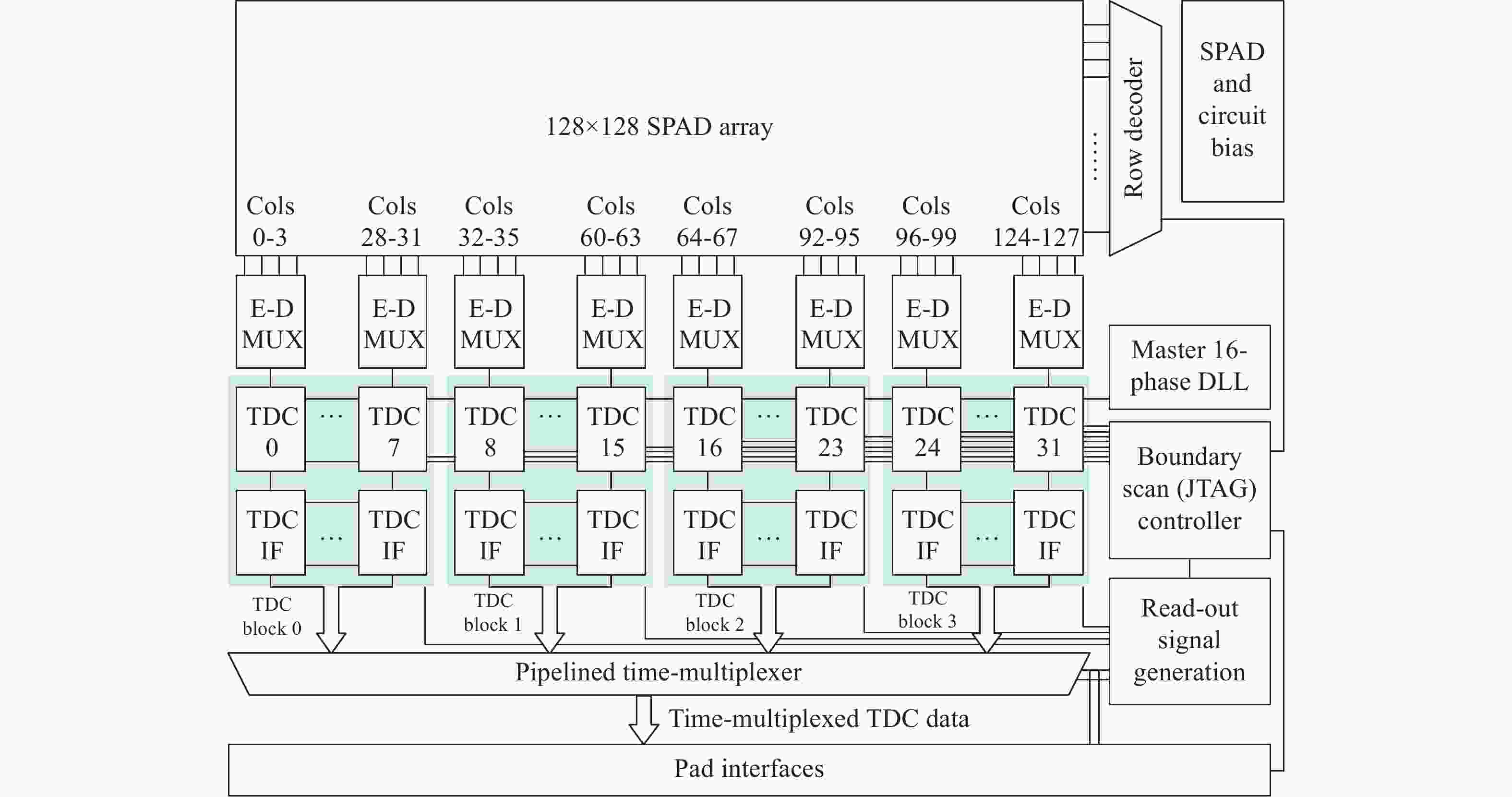
图 5 基于TDC共享方案的ROIC架构
Figure 5. ROIC architecture based on TDC sharing scheme
TDC共享方案通过减少系统中TDC的个数来实现低功耗,同时TDC面积不受单个像素单元的限制,因此可以采用多段式TDC、时间放大等方法改善时间分辨率。TDC共享方案可以兼顾功耗与精度,但牺牲了成像分辨率和检测效率。共享架构导致使用同一个TDC的像素每帧只能探测一个返回光子,因此TDC共享技术主要适用于成像帧频要求不高、光子稀疏的特定应用场合。
-
与基于TOF测量的ROIC不同,基于光子计数的ROIC在一个曝光时间内可以对光子到达信号进行多次检测。单位曝光时间内检测到的光子数量对应了不同的目标灰度信息,因此该类电路主要用于灰度成像。
光子计数读出电路的基本性能指标为阵列规模,像素面积、计数动态范围。像素面积越小,分辨率越高,成像质量越好。计数动态范围则是指一帧曝光内能检测到的光子个数的范围,动态范围受像素面积的限制。表2为光子计数读出电路的主要研究进展。
表 2 光子计数读出电路研究进展情况
Table 2. Research progress of photon counting readout circuit
Year 2015[23] 2020[24] 2022[25] 2019[26] 2021[27] Institution MIT Lincoln
LaboratoryOregon State
UniversityUniversity of
EdinburghTechnion-Israel
Institute of
TechnologySoutheast
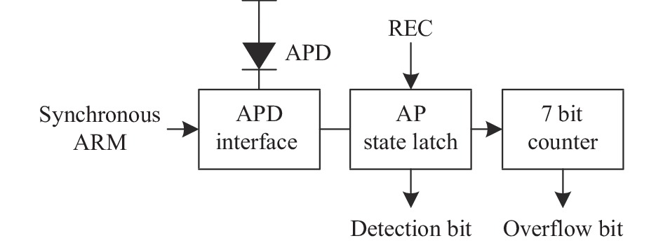
UniversityTechnology 0.18 μm CMOS 0.18 μm CMOS 40 nm CMOS 0.18 μm CMOS 0.18 μm CMOS Pixel array 256×256 8×8 128×120 64×64 128×1 Pixel pitch 25 μm 80 μm 8 μm 25 μm 80 μm Dynamic range 42 dB 129 dB 126 dB - 60 dB 2015年,林肯实验室提出了一种基于硅盖革模式雪崩光电二极管(Geiger-mode Avalanche Photodiode, GM-APD)的256×256光子计数系统 [23]。该系统将一种硅GM-APD阵列与数字CMOS计数芯片混合集成,其单像素结构框图如图6所示,由APD探测器、APD接口电路、APD状态锁存器和7 bit计数器构成。像素中心距为25 μm,所有探测器的阳极被统一施加偏置电压,通过全局同步的脉冲信号来调控APD探测器的工作状态。

图 6 256×256光子计数系统的单像素结构框图
Figure 6. Single pixel structure block diagram of 256×256 photon counting system
由于每个像素接受到的光子个数不同,因此,每个像素都具有光子计数功能,可以对雪崩信号进行计数。理论上探测器在检测到光子并雪崩淬灭后,应立即复位以便准备下一次检测。但是,受探测器性能的限制,即连续工作会导致探测器的后脉冲发生率和暗计数率较高,所以还要加入探测器死区时间调节电路。死区时间的选取和确定需要综合多种因素,包括光子密度分布、光子探测率、精度、曝光时间、最大计数率等等,从而在不同光强条件下均能实现高精度的光子计数及数据读出。因此,在该类电路中,死区时间的调节方法是一个较为关键的技术。
2019年,东南大学提出一种光子时间自适应调节的读出电路结构,在电路系统中设置了判断电路,将一帧内检测到的光子个数与最佳死区时间存储于电路内,在实时检测光子过程中,对光子个数进行判断并与芯片内存储的死区时间进行对比,实时调节SPAD的死区时间,达到了最优的探测率。
光子计时是通过TDC对光子的飞行时间直接测量,在有限像素面积下,TDC精度和量程受到制约,且随着阵列规模扩大,TDC功耗会成倍增加。目前主流的解决方法是TDC共享,多个像素共享同一个TDC,节省了面积和功耗,但也带来了检测效率下降、成像分辨率下降的问题。光子计数是在像素中内置计数器,对探测到的光子计数。由于计数器不像TDC需要同时保证精度和量程,计数器所占的面积要远小于TDC,光子计数受到的像素面积的制约较小。但光子计数要求电路能够自恢复SPAD,这面临着后脉冲和暗计数问题,如何在保证探测效率的同时,最小化SPAD的后脉冲和暗计数是光子计数面临的关键问题。
-
传统ROIC的主要功能包括雪崩电流的检测与淬灭、光子飞行时间的测量或返回光子个数的计数、数据输出。数据的存储和处理一般在片外进行。随着阵列规模的扩大、数据量的增加,ROIC的功能也变得更加丰富。近年来主要新出现了以下几个趋势:
(1) 片上数据存储。一般ROIC的像素内的寄存器是复位的,作为TDC将TOF进行量化,同时将量化后的数据进行存储传输,因此在一帧成像中量化后的数据需要实时传输到芯片外。随着阵列规模的增大,数据量急剧增加,但是由于数据传输速度和数据端口数量的限制,传统的数据传输方案越来越成为限制成像帧频提高的主要因素,片上存储技术因此应运而生[18,28]。此类ROIC一般将若干个TDC编为一组,每组共享一个片上存储单元。当像素检测到光子触发信号后,TDC会将量化后的数据缓存至片上存储单元,不再占用像素内的寄存器,将数据量化与传输进行分离。片上数据存储技术极大地减小了数据读出时间对系统帧频的限制,使系统能够达到很高的帧频。然而该技术需要在电路中设计相应的静态随机存取存储器(Static Random Access Memory, SRAM)。还需要解决如何对像素阵列空间进行仲裁、寻址,如何将TDC中的数据写入存储单元、再有序读出等问题,数字时序复杂,需要相关电路的精密配合。
(2) 返回光子事件多回波探测。由于传统的基于TOF测量的成像系统在每一帧曝光时间内,最多只检测一次返回光子,并且暗计数和空气中颗粒物等因素导致像素的虚假探测率较高,所以很容易出现像素在一帧内发生了一次虚假检测并停止继续检测的情况。ROIC检测到的大量雪崩信号并不是目标光子回波产生的,而是其他因素造成的虚假回波,这也是导致SPAD阵列的实际成像帧频无法提升的主要因素之一。多回波探测技术使ROIC在一帧内可以检测两次或以上的光子回波,并测量对应的TOF[29]。这就提高了每一帧检测到目标光子回波的概率,也便于利用目标光子回波的时空相关性快速筛选出有效数据。多回波探测技术带来的问题是寄存器数量倍增以及逻辑控制电路更加复杂,这在像素面积严格限制的ROIC电路中是一个需要折中取舍的问题,因此在实际应用中,多回波检测电路需要与像素共享或片上存储等架构一起使用,才能实现多次回波检测。
(3) 自由探测模式。迄今为止,门控模式能够满足三维激光雷达在内的大部分应用,但其固定时间间隔使能的操作方式也将SPAD探测器的曝光时间限制在了门控信号与激光信号同步的低占空比应用中。为了将SPAD探测器应用在连续光子事件探测场景中,工作在自由探测模式的SPAD阵列读出电路近年被开发[30]。自由探测模式中,各探测器工作于自由模式,相互独立、不受统一的门控信号控制。探测器可以在待测、淬灭状态之间自由切换,并为每次探测到的光子事件记录时间戳。为保证探测的连续,所记录的时间戳数据还需进行实时读出。自由探测模式的时序逻辑控制比门控模式更复杂,电路功耗和面积也更大。2017年,普林斯顿光波公司Merlin实验室研制了一款运行在自由探测模式下的读出电路,像素规模为32×32,采用蜂窝状非常规像素布局,像元中心距为66 μm[31]。自由探测模式读出电路控制复杂,精度要求高,电路功耗较传统门控模式大大提高,成为限制自由探测模式阵列扩大的一个主要因素,因此,自由探测模式目前阵列规模较小,像素面积也较大。
-
纵观国内外SPAD阵列读出电路的发展,电路的性能在提升,但是其提升速度远不及其他集成电路。主要的原因是随着阵列规模的增大,电路功耗成比例增加,尤其对于普遍需要制冷的SPAD探测器来说,此类问题影响更为严重,成为限制SPAD面阵规模进一步扩大的主要因素。事件驱动型TDC、像素共享型TDC的架构提出解决了一部分的功耗问题,但是随着ROIC时间分辨率精度要求的提升,电路工作频率的提高,以及电路功能的增加,功耗仍是一个较难解决的问题。其次,SPAD探测器由于极高的增益,易产生暗计数,而暗计数引起的雪崩与光计数类似,电路难以区分,导致电路TOF的量化数据是大量的无效数据,需要多帧检测进行数量融合,实际成像速度非常低。如何在电路硬件中融合去噪算法,也是今后读出电路需要重点解决的问题。
随着SPAD阵列应用需求的进一步发展,读出电路将集成更多的功能,进一步向感、存、算一体化方向发展,最终真正实现单芯片成像。
Key technologies and development trends of SPAD array readout circuit (invited)
-
摘要: 首先针对SPAD阵列读出电路的特点,将电路主要分成接口电路与信号处理电路两大部分,其次根据单光子雪崩光电探测器的阵列的不同应用场景,阐述了集成读出电路中核心电路模块设计的关键技术。分别从SPAD的接口电路设计、两种典型应用成像模式(光子计时、光子计数)中核心电路的设计方面,详细分析此类电路的关键技术以及国内外研究团队在此类电路的研究进展与存在的问题。最后根据目前国内外研究的进展情况,分析了SPAD阵列集成读出电路的发展趋势以及各类电路存在的设计重点与难点,为SPAD阵列读出电路的设计提供一些参考。Abstract:
Significance In recent years, the Single Photon Avalanche Diode(SPAD) with single-photon detection capability has been widely used in weak light detection fields such as laser radar, quantum communication, fluorescence spectrum analysis and so on because of its advantages of high sensitivity, fast response, strong anti-interference ability and small size. As a new nonlinear device, SPAD detector has complex manufacturing process. In addition, various applications of SPAD array need readout integrated circuits (ROIC) for detecting sensing signals to be matched with them to achieve the extraction and processing of SPAD detector avalanche signals. Various applications have increasingly high requirements for array size, detector signal extraction and processing capabilities. At the same time, the parasitic effect, power consumption, area and other problems caused by large-scale array are becoming more and more prominent, which seriously affects the imaging quality. The design of array-type SPAD readout circuit is facing great challenges. Progress The readout circuit of SPAD array is mainly composed of interface circuit and signal processing circuit. The interface circuit realizes the quenching and extraction of avalanche signal, and the switching between the cut-off and the state to be measured of SPAD. It is a dynamic bias circuit. With the expansion of the array scale, it is required to add SPAD anti-bias voltage adjustable circuit in the interface circuit, realize pixel-by-pixel or regionally adjustable bias of SPAD, and SPAD high-voltage breakdown protection circuit. At present, such technology is only used in small-scale, linear array and some applications, but still cannot be realized in the application of large area array. The main difficulty is that complex circuits cannot be used due to the limitation of pixel area. According to the application of SPAD, the signal processing circuit is divided into photon timing circuit and photon counting circuit. The photon timing circuit is used to measure the flight time of photons. In the circuit, the array-type time-to-digital conversion circuit (TDC) is used. Because the arrival time of each pixel is different, each pixel needs an independent TDC, and the circuit power consumption is very high. This is also one of the reasons that limit the scale expansion of SPAD array. A related research team has proposed a TDC sharing structure, such as the Lausanne Institute of Technology in Switzerland, which proposed a TDC sharing structure (Fig.3). At the same time, because the pixel area is not limited by sharing, multi-segment TDC can be used, and the time resolution of the circuit is less than 100 ps. Compared with the photon timing circuit, the structure of the photon counting circuit is relatively simple. It only needs to record the number of photons detected in a frame. The difficulty of this kind of circuit is to effectively adjust the dead time of the SPAD detector to achieve the best compromise between the detection rate and the dark count. Conclusions and Prospects With the demand for SPAD large arrays and the development of readout circuits, the following development trends have emerged in relevant readout circuits in recent years: on-chip data storage, multiple echo detection of returned photon events, and free detection mode. With the further development of the application requirements of SPAD array, the readout circuit will integrate more functions, further develop towards the integration of sensing, memory and computing, and finally truly realize single-chip imaging. -
图 1 (a)被动淬灭电路; (b)主动淬灭电路
Figure 1. (a) Passive quenching circuit; (b) Active quenching circuit
图 6 256×256光子计数系统的单像素结构框图
Figure 6. Single pixel structure block diagram of 256×256 photon counting system
表 1 光子计时读出电路的性能对比
Table 1. Performance comparison of photon timing readout circuit
Year 2018[18] 2020[19] 2020[20] 2018[21] 2019[22] Institution MIT Lincoln Laboratory University of Edinburgh Swiss Federal Institute of Technology Delft University of Technology Southeast University Technology 0.18 μm CMOS 40 nm CMOS 0.35 μm CMOS 0.18 μm CMOS 0.18 μm CMOS Pixel array 256×128 128×128 32×128 252×144 64×64 Pixel pitch 50 μm 40 μm×20 μm 40 μm 28.5 μm 50 μm TDC resolution 500 ps 100 ps 78 ps 48.8 ps 1000 ps TDC range - 23.3 ns 640 ns 333 ns 4000 ns Frame rate - 500 fps 20 fps 31.25 kfps 20 kfps Power - 185 mW - 2540 mW 490 mW  下载: 导出CSV
表 2 光子计数读出电路研究进展情况
Table 2. Research progress of photon counting readout circuit
Year 2015[23] 2020[24] 2022[25] 2019[26] 2021[27] Institution MIT Lincoln
LaboratoryOregon State
UniversityUniversity of
EdinburghTechnion-Israel
Institute of
TechnologySoutheast
UniversityTechnology 0.18 μm CMOS 0.18 μm CMOS 40 nm CMOS 0.18 μm CMOS 0.18 μm CMOS Pixel array 256×256 8×8 128×120 64×64 128×1 Pixel pitch 25 μm 80 μm 8 μm 25 μm 80 μm Dynamic range 42 dB 129 dB 126 dB - 60 dB
下载: 导出CSV
-
[1] Deshpande R R, Bhatt M R, Madhavi C H R. Accuracy in depth recovery and 3D image synthesis from single image using multi-color filter aperture and shallow depth of field [J]. IEEE Access, 2021, 9(9): 123528-123540. [2] Kang Y, Xue Ruikai, Li Lifei, et al. Continuous scanning 3D imaging with SPAD array based on pixel multiplexing [J]. Infrared and Laser Engineering, 2020, 49(S2): 20200375. (in Chinese) doi: 10.3788/IRLA20200375 [3] Jin Chenfei, Tian Xiaorui, Tang Meng, et al. Research advances on non-line-of-sight three-dimensional imaging lidar [J]. Infrared and Laser Engineering, 2022, 51(3): 20210471. (in Chinese) doi: 10.3788/IRLA20210471 [4] Guo H B, He X W, Liu M H, et al. Three-dimensional radiopharmaceutical-excited fluorescence imaging of lymph nodes[C]//IEEE Nuclear Science Symposium & Medical Imaging Conference, 2017: 1-3. [5] Vornicu I, Carmona-Galan R, Rodriguez-Vazquez A. On the calibration of a SPAD-based 3D imager with in-pixel TDC using a time-gated technique[C]//IEEE International Symposium on Circuits & Systems, 2015: 1102-1105. [6] Zhu Y J, Niu Y Z, Lu W G, et al. A 160×120 ROIC with non-uniformity calibration for silicon diode uncooled IRFPA[C]//2019 IEEE International Conference on Electron Devices and Solid-State Circuits, 2019: 1-3. [7] Perenzoni M, Massari N, Gasparini L, et al. A fast 50×40-pixels single-point DTOF SPAD sensor with photon counting and programmable ROI TDCs, with σ<4 mm at 3 m up to 18 klux of background light [J]. IEEE Solid-State Circuits Letters, 2020, 3: 86-89. doi: 10.1109/LSSC.2020.3005760 [8] Ameri M, Kamrani E, Hashemi S, et al. A fast quench-reset integrated circuit for high-speed single photon detection[C]//2013 IEEE International Symposium on Medical Measurements and Applications, 2013: 179-182. [9] Tosi A, Mora A D, Zappa F, et al. Single-photon avalanche diodes for the near-infrared range: Detector and circuit issues [J]. Journal of Modern Optics, 2009, 56(2-3): 299-308. doi: 10.1080/09500340802263075 [10] Tisa S, Zappa F, Tosi A, et al. Electronics for single photon avalanche diode arrays [J]. Sensors and Actuators A Physical, 2007, 140(1): 113-122. doi: 10.1016/j.sna.2007.06.022 [11] Zappa F, Ghioni M, Cova S, et al. An integrated active-quenching circuit for single-photon avalanche diodes [J]. IEEE Transactions on Instrumentation & Measurement, 2000, 49(6): 1167-1175. [12] Chang P H, Tsai C M, Wu J Y, et al. Constant excess bias control for single-photon avalanche diode using real-time breakdown monitoring [J]. IEEE Electron Device Letters, 2015, 36(8): 859-861. doi: 10.1109/LED.2015.2450936 [13] Zheng Lixia, Zhang Guangchao, Tian Jiangjiang, et al. An integrated bias voltage control method for SPAD arrays [J]. IEEE Photonics Technology Letters, 2018, 30(19): 1723-1726. [14] Deng S J, Declan G, Morrison A P. A Geiger-mode APD photon counting system with adjustable dead-time and interchangeable detector [J]. IEEE Photonics Technology Letters, 2016, 28(1): 99-102. doi: 10.1109/LPT.2015.2487342 [15] Wang H C, Dai F F. A 14-bit, 1-ps resolution, two-step ring and 2D vernier TDC in 130 nm CMOS technology[C]//43rd IEEE European Solid State Circuits Conference, 2017: 143-146. [16] Ferreira L, Moreira M B, Souza B, et al. Review on the evolution of low-power and highly-linear time-to-digital converters-TDC[C]//2020 IEEE 11th Latin American Symposium on Circuits & Systems, 2020: 1-4. [17] Niclass C, Favi C, Kluter T, et al. A 128×128 single-photon image sensor with column-level 10-bit time-to-digital converter array [J]. IEEE Journal of Solid-State Circuits, 2008, 43(12): 2977-2989. doi: 10.1109/JSSC.2008.2006445 [18] Aull B F, Duerr E K, Frechette J P, et al. Large-format Geiger-mode avalanche photodiode arrays and readout circuits [J]. IEEE Journal of Selected Topics in Quantum Electronics, 2018, 24(2): 1-10. [19] Mattioli Della Rocca F, Mai H, Hutchings S W, et al. A 128 × 128 SPAD motion-triggered time-of-flight image sensor with in-pixel histogram and column-parallel vision processor [J]. IEEE Journal of Solid-State Circuits, 2020, 55(7): 1762-1775. doi: 10.1109/JSSC.2020.2993722 [20] Jahromi S, Jansson J P, Kernen P, et al. A 32×128 SPAD-257 TDC receiver IC for pulsed TOF solid-state 3-D imaging [J]. IEEE Journal of Solid-State Circuits, 2020, 55(7): 1960-1970. doi: 10.1109/JSSC.2020.2970704 [21] Zhang C, Lindner S, Ivan Michel Antolović, et al. A 30-frames/s, 252×144 SPAD flash LiDAR with 1728 dual-clock 48.8-ps TDCs, and pixel-wise integrated histogramming [J]. IEEE Journal of Solid-State Circuits, 2019, 54(4): 1137-1151. doi: 10.1109/JSSC.2018.2883720 [22] Wu Jin, Qian Zhiming, Zhao Yang, et al. 64×64 GM-APD array-based readout integrated circuit for 3D imaging applications [J]. Science China Information Sciences, 2019, 62(6): 062407:1-062407:11. [23] Aull B F, Schuette D R, Young D J, et al. A study of crosstalk in a 256×256 photon counting imager based on silicon Geiger-mode avalanche photodiodes [J]. IEEE Sensors Journal, 2015, 15(4): 2123-2132. doi: 10.1109/JSEN.2014.2368456 [24] Ouh H, Shen B, Johnston M L. Combined in-pixel linear and signal-photon avalanche diode operation with integrated biasing for wide-dynamic-range optical sensing [J]. IEEE Journal of Solid-state Circuits, 2020, 55(2): 392-403. doi: 10.1109/JSSC.2019.2944856 [25] Erdogan A T, Al Abbas T, Finlayson N, et al. A high dynamic range 128×120 3-D stacked CMOS SPAD image sensor SoC for fluorescence microendoscopy [J]. IEEE Journal of Solid-State Circuits, 2022, 57(6): 1649-1660. doi: 10.1109/JSSC.2022.3150721 [26] Katz A, Shoham A, Vainstein C, et al. Passive CMOS single photon avalanche diode imager for a gun muzzle flash detection system [J]. IEEE Sensors Journal, 2019, 19(14): 5851-5858. doi: 10.1109/JSEN.2019.2904312 [27] Zheng Lixia, Guo Pengcheng, Lu Hai, et al. An ultraviolet photon counting imaging system based on a SiC SPAD array [J]. IEEE Photonics Technology Letters, 2021, 33(21): 1213-1216. doi: 10.1109/LPT.2021.3113181 [28] Augusto R X, Preethi P, Myung-jae L, et al. A modular, direct time-of-flight depth sensor in 45/65-nm 3-D-stacked CMOS technology [J]. IEEE Journal of Solid-State Circuits, 2019, 54(11): 3203-3214. doi: 10.1109/JSSC.2019.2938412 [29] Xu W S, Zhen S W, Xiong H L, et al. Design of 128×32 GM-APD array ROIC with multi-echo detection for single photon 3D LiDAR[C]//SPIE Seventh Symposium on Novel Photoelectronic Detection Technology and Application, 2021, 11763: 117634A. [30] Glettler J B, Hopman P I, Verghese S, et al. InP-based single-photon detector arrays with asynchronous readout integrated circuits [J]. Optical Engineering, 2008, 47(10): 100502. doi: 10.1117/1.2992138 [31] Itzler M, Salzano G, Entwistle M, et al. Asynchronous Geiger-mode APD cameras with free-running InGaAsP pixels[C]//SPIE Commercial+Scientific Sensing and Imaging, 2017, 10212: 102120K. -

 点击查看大图

计量
- 文章访问数: 295
- HTML全文浏览量: 115
- PDF下载量: 182
- 被引次数: 0

