


-
透明硬脆材料是指一类硬度高、脆性大、断裂韧性低的透明材料,通常为非金属材料。由于其硬度高、热稳定性好、抗腐蚀能力强以及优异的光电特性[1-4],广泛应用于半导体、电子、航空航天和新能源等领域[5-6]。硬脆材料切片是相关器件制备的关键环节之一,由于材料高硬度和高脆性的特点,使得传统的机械加工,如金刚线锯割工艺容易在材料表面和内部产生微裂纹、杂质颗粒和重熔层等损伤,切片效率、材料利用率、以及良率较低,严重制约了硬脆材料推广应用。
脉冲激光尤其是超快激光具有较高的峰值功率[7],脉冲宽度接近或小于材料热弛豫时间,是加工脆性材料的理想选择,具有非接触、高效率、高精度、低损耗等优势。特定波长的激光可以透过透明硬脆材料,利用透镜将光束聚焦在材料内部,通过控制光束的运动轨迹,在透明硬脆材料内部形成含空隙、高密度位错、微裂纹等微缺陷的改质层[8],在热应力或外载荷作用下沿改质层,并垂直激光入射方向发生剥离,实现材料切片。激光剥离为透明硬脆材料切片提供了一种全新的工艺方法,成为目前激光应用领域的研究热点。
文中从透明硬脆材料激光剥离工艺的物理过程出发,讨论激光剥离过程的关键科学问题,并综述了近年来激光剥离透明硬脆材料的研究进展,并提出未来的潜在发展方向。
-
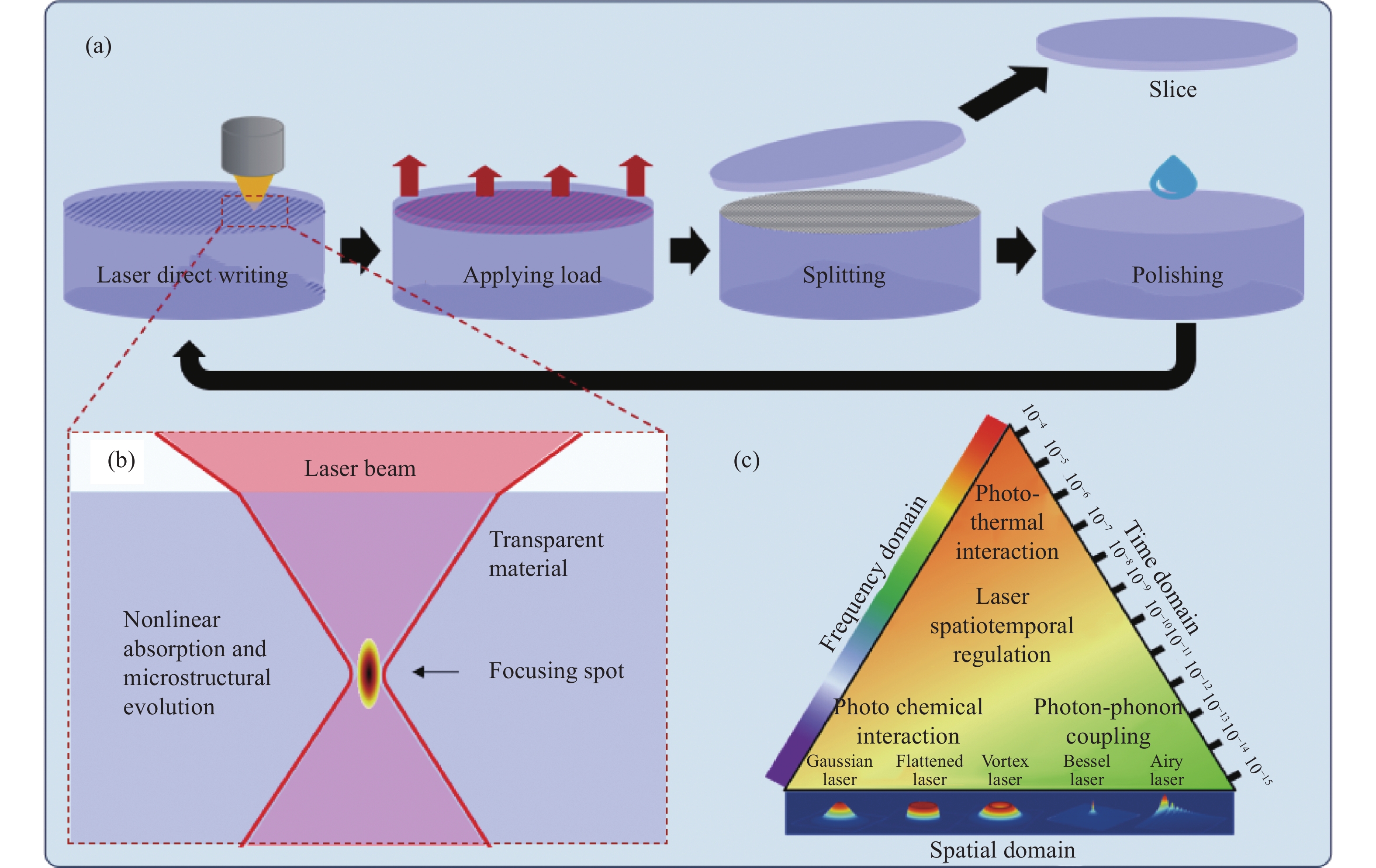
激光剥离硬脆材料过程如图1(a)所示,激光作用于材料内部,形成一层厚度为数微米到数十微米的改质层,改质层中包含微裂纹等微缺陷[9]。通过外载荷拉伸材料,使材料沿着微裂纹拓展方向剥离。激光束路径上未聚焦处,由于激光能量密度小于材料损伤阈值,未聚焦区域材料无损伤,从而实现透明硬脆材料特定位置改质切片。剥离后对剩余材料表面抛光,去除激光改质层表面及亚表面缺陷,准备下一次的激光剥离。

图 1 (a)硬脆透明材料激光剥离过程示意图;(b)激光剥离过程焦点位置非线性吸收;(c)激光光场时空调控
Figure 1. (a) Schematic diagram of laser separate; (b) Nonlinear absorption and microstructure evolution during laser separate; (c) Laser spatiotemporal regulation
如图1(b)、(c)所示,激光剥离过程关键的科学问题包括透明硬脆材料对激光的非线性吸收,激光作用下透明硬脆材料内部微观结构演化,以及激光光场调控对材料改质影响机制等。对这些问题的深刻认识有助于工艺优化,提升激光剥离质量。
-
激光剥离的关键因素之一是确定激光在材料内部聚焦的焦点位置,这需要深入研究透明硬脆材料对激光的非线性吸收机理。激光聚焦于透明材料内部,发生多光子吸收[10],由光子能量计算公式E=hc/λ可知,光子能量与激光波长成反比。因此,需要选择光子能量小于材料禁带宽度的激光波长,确保激光能量不破坏材料表面和聚焦路径上的材料内部区域。常见透明硬脆材料属性如表1所示。
表 1 典型透明硬脆材料属性
Table 1. Typical transparent hard brittle material properties
Materials Melting temperature/K Boiling temperature/K Band gap/eV Moh's hardness Si[11] 1690 3540 1.10 7.0 SiC[12-14] 2970 3770 3.26 9.5 GaN[15] 1 973 2676 3.40 9.2 Fused silica[16-17] 1 986 3100 9.00 7.0 sapphire[18] 2350 3770 9.90 9.0 Diamond[19-20] 4750 5100 5.50 10 KDP[21-22] 451 653 5.91 2.5 YAG[23-24] 2220 2510 6.50 8.5 Lu2O3[25-26] 2760 4250 5.80 7.0 Y2O3[25, 27] 2690 4570 5.60 8.5 多光子吸收通常发生于超快激光制造过程。激光聚集在材料表面或内部,发生了一系列复杂的能量弛豫过程,引发了复杂的非线性效应产生[28]。1987年,Srinivasan等[29]首次将超快激光应用于材料加工。飞秒激光超短时间内将激光能量耦合到材料中,材料内部在焦点处产生非线性吸收,仅对材料局部作用[30]。超快激光与物质相互作用包括几种不同机制:载流子激发[31]、热匀化[32]、热效应[33]和结构效应[34]。超快激光的高峰值功率密度使焦点附近发生多种电离[35]。当激光能量低时,主要是多光子吸收电离[36],价带电子会同时吸收多个光子,从价带跃迁至导带。当激光能量密度高时,则主要发生隧穿电离[37]。电子通过隧穿效应直接从价带跃迁至导带。当自由电子吸收大量能量达到一定阈值时,碰撞其他离子,使自由电子密度快速增大,发生雪崩电离[38]。由于透明硬脆材料本身几乎没有自由电子,超快激光非线性电离过程中产生的自由电子会为雪崩电离提供种子。电离完成后自由电子通过散射重新分布实现热匀化,激光能量经过非线性吸收和声子传递导致激光焦点区域材料受热熔化或断裂,结构发生永久性改变。通过热扩散,材料温度在微秒的时间尺度上恢复,多余的载流子通过电子和空穴的复合或从激发区扩散而消除[39-40]。
-
激光聚焦在材料内部累积能量,导致其发生多种结构变化。较低能量密度的激光与材料发生复杂非线性作用,使材料受到永久性损伤,材料折射率发生改变[41-42],如图2(a)所示。对于玻璃材料,激光能量使玻璃材料化学键断裂或者键角发生改变,实现激光聚焦区域材料的致密化,导致材料折射率增大[43]。对于晶体材料,激光聚焦区域局部形成空化效应,导致晶体材料局部密度变小,折射率减小[44]。
当激光能量适中时,超快激光烧蚀材料内部会产生与激光偏振特性密切相关的纳米光栅结构。Mysyrowicz等[45]研究了石英玻璃激光烧蚀后出现双折射率各向异性改变,研究表明,激光能量超过一定阈值时,材料产生纳米光栅结构,如图2(b)所示。目前,相关机理解释有激光诱导等离子体与入射激光光场干涉机制[46]、纳米等离子体基元各向异性膨胀机制[47]和缺陷辅助纳米条纹形成机制[48]等。
高峰值功率超快激光聚焦在一个很小的体积内,导致材料内部产生多光子电离与雪崩电离,发生微爆炸现象[49],产生极端压力,聚焦区温度瞬间提高,将材料温度提升至汽化温度以上,硬脆材料蒸汽在材料内部发生蒸汽拓展,强烈的冲击拓宽激光作用范围,压缩周围物质,形成一种有孔隙、高位错密度层以及裂纹的改质层。该条件下聚焦区域产生高温高压环境,诱导物质转变为另一种相,并最终在聚焦区域产生纳米孔洞[50],如图2(c)所示。
较大能量密度激光与物质相互作用过程中,脉冲激光在材料内产生较高峰值温度,使材料焦点处产生爆炸性气体,气体膨胀产生压缩应力波,在材料内产生拉伸应力,当应力超过材料强度时,在其内部形成裂纹,辅助改质层裂纹在水平方向上扩展[10],如图2(d)所示。
数值仿真是研究激光与透明硬脆材料相互作用过程的有效方法[54-57],Etsuji Ohmura等[55]数值模拟了硅晶圆激光隐切过程单脉冲激光作用下材料内部的温度历程,如图3所示。通过计算结果与试验测试对比,发现硅晶圆材料对激光的吸收系数受材料温度影响,吸收系数随温度上升而增加,研究结果显示硅晶圆材料内部温度约2000 K时形成高位错密度层,温度超过10000 K时材料会瞬间汽化形成孔洞。王文君等[56]利用800 nm波长飞秒激光对碳纤维增强碳化硅材料进行加工工艺研究,通过计算碳化硅材料表面的电场分布,解释了微观形貌成形机制,研究发现,飞秒激光在碳化硅不同位置发生衍射和反射,导致表面电场漂移和损耗,并由此造成碳化硅烧蚀区域微槽弯曲和宽度不均匀现象。

-
激光剥离过程,改质层的厚度决定了材料损耗与后期磨抛工作量,通过光场调控能够提高激光加工轴向分辨率,降低改质层厚度,提升材料剥离的质量与效率。
Valentina等[58]提出的时空协同调控飞秒激光时空聚焦技术如图4所示。通过将飞秒激光脉冲调控,实现激光脉冲在时间上被拉长,降低脉冲峰值功率。当脉冲接近焦点时,所有组成的波长重新结合,脉冲缩短,在焦点位置脉宽最短,形成峰值功率最高的激光脉冲。在焦点处获得最短的脉宽有助于加强对多光子激发的调控。

激光在透明硬脆材料内部聚焦引起的像差降低了轴向加工分辨率,可通过位于物镜之前的自适应光学元件对激光束施加相反的相位,如空间光调制器(SLM)等,消除向焦点方向传播的像差,如图5所示[59]。Salter等[60]利用SLM在熔融石英中进行像差校正来提高超快激光的加工精度,相比于无像差校正时,聚焦位置精度得到显著改善。Yasuhiko Shimotsuma等[61]发现高数值孔径物镜在SiC剥离实验中产生严重的球差效应,光斑在轴向上明显拉伸,能量呈椭圆状分布。该团队搭建了Mach-Zehnder型双脉冲激光光路,采用SLM补偿由于SiC高折射率造成的球差,减小晶圆剥离所需应力到原来的十分之一。
-
激光多脉冲时域整形的主要目标是调整激光脉冲的时间特性,如子脉冲个数、脉冲宽度、脉冲间隔、相位等,以获得所需的激光脉冲序列输出。激光时域整形技术在透明硬脆材料加工领域展现出显著优势[62]。
Hernandez-Rueda等[63]对飞秒脉冲序列激光微纳加工开展研究,通过空间光调制器改变激光脉冲数量、序列及其单个脉冲宽度,研究了整形脉冲激光对融石英表面烧蚀孔洞的影响,相对于未整形的脉冲,时域整形脉冲很容易加工出小于50 nm深度的表面微结构。姜澜等[64]研究发现,时域整形脉冲序列可以改变熔融石英周期性条纹的方向,这为通过时域整形脉冲序列制备不同周期的光栅提供了可能性。朱健强等[65]研究了1053 nm、脉宽8.9 ps双脉冲激光时域整形系统,对K9玻璃烧蚀特性进行分析,研究发现双脉冲产生冲击波干涉,形成环状烧蚀结构,子脉冲间隔对烧蚀阈值和烧蚀效率具有显著影响。
-
多焦点扫描是常用的分布式激光光场整形技术之一,是指一次生成多个光束聚焦点来进行透明硬脆材料的改质,提升激光能量利用率。生成多焦点激光的方式多采用透镜阵列组和空间光调制器生成。
匡翠方等[66]基于空间光调制器与多通道声光调制器产生六束飞秒激光光束,且每束光的开关与光强皆可以独立控制,如图6所示。
张雷等[67]设计了4×4矩形排列的光点阵列,得到分辨率1024×1024的全息图,导入SLM中。采用飞秒激光全息处理系统在蓝宝石表面制备透镜阵列,激光加工速度高达每分钟9600个凹坑,为蓝宝石基光学器件的高效制造开辟了新途径。
-
传统硬脆材料切片采用金刚线切割工艺,切割损耗大且材料表面损伤严重[68-69]。超快激光加工透明硬脆材料采用无接触切割方式,获得的成品无裂痕且切面整齐平滑。下文针对不同种透明硬脆材料的剥离加工进行论述。
-
SiC是典型的第三代半导体材料,SiC晶体有许多种多型,迄今为止被确认的多型多达200余种,其中4H-SiC多型具有较高的本征载流子浓度和电子迁移率,被广泛用于电力电子功率器件[70]。由于硬度极高,传统金刚线切片难度大,导致晶圆成本高。4H-SiC晶圆激光剥离成为近年来的激光应用的研究热点。
2016年,德国Siltectra公司在SiC晶圆及相关材料欧洲会议[71] (2016 European Conference on Silicon Carbide & Related Materials, ECSCRM) 上提出了一种名为“COLD SPLIT”SiC晶圆切片技术,如图7所示。2018年11月,德国Infineon公司耗资1.24亿欧元收购了Siltectra公司。
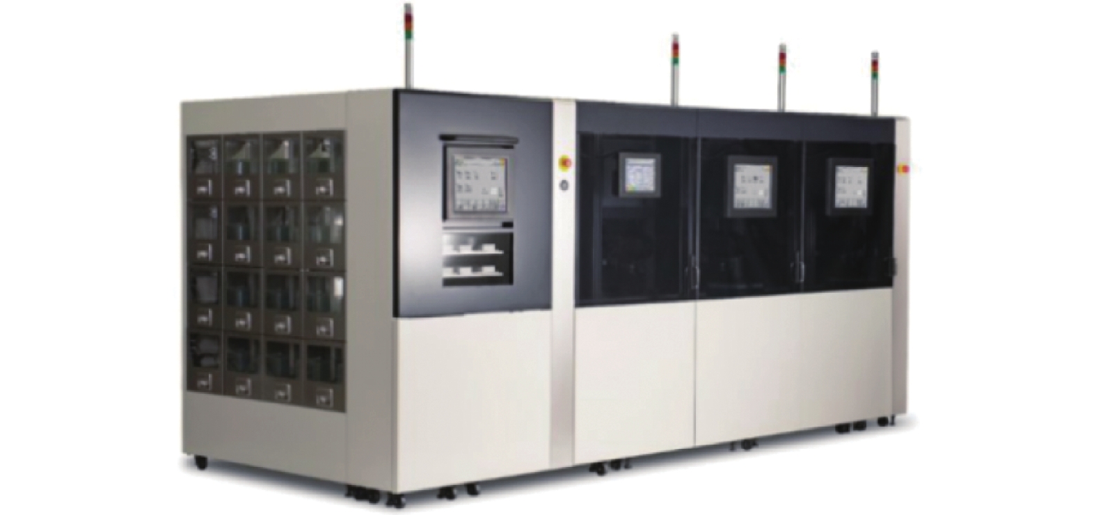
2018年,在SPIE会议上,日本Disco公司的Kazuya Hirata[72]公布了一种名为“KABRA”的工艺,使用激光加工技术的新晶圆生产工艺研制了自动剥离设备,如图8所示。现有工艺需约3 h才能实现6 in (1 in=2.54 cm) SiC晶锭切片。相比之下,KABRA工艺可大大缩短晶圆剥离时间,该技术可以精确地将350 μm厚SiC晶圆在10 min内剥离。
国内方面,2022年,林学春等[10]将1064 nm、12.6 ps皮秒激光聚焦到4H-SiC晶圆内部,SiC在激光的瞬间高温作用下形成一层孔隙、高位错密度层以及裂纹组成的改质层,500 μm的4H-SiC晶圆通过机械拉伸剥离为两个厚度250 μm的薄晶圆,粗糙度为1.8 μm,如图9所示。王荣堃等[73]通过激光切片对具有不同表面粗糙度的4H-SiC样品进行了处理,研究结果表明,良好的表面质量可以减少激光切片过程中对晶片表面的损伤,提高改性层的平整度和均匀性。谢小柱等[74]利用皮秒脉冲激光改质SiC,做到剥离后SiC损伤层小于100 μm。

王蓉等[75]提出了一种飞秒激光辐照与带隙选择性光电化学剥离复合方法,将激光扫描改质后的SiC通过电解液的选择性刻蚀作用选择性刻蚀改质层,刻蚀后的SiC样品保持原有特性不变且上下层完整,剥离过程如图10所示。

国内产业化方面,深圳市大族半导体装备科技有限公司[76]、苏州德龙激光股份有限公司[77]、北京晶飞半导体科技有限公司、西湖仪器(杭州)技术有限公司[78]等在SiC晶圆激光剥离技术方面取得了显著进展,并研制出能够剥离8 in SiC晶锭的激光剥离装备,相关设备主要技术参数如表2所示。
表 2 SiC晶锭激光切片设备主要参数
Table 2. Main parameters of SiC ingot laser slicing equipment
Shenzhen Han's Semiconductor Equipment Technology Co., Ltd[76] Westlake Instruments (Hangzhou) Technology Co., Ltd[78] Maximum cutting size SiC material, 8-inch downward compatible Processing dimensions SiC material, 4/6/8 in Ingot thickness - Ingot thickness ≤50 mm
(customizable)Maximum cutting thickness 5 mm Slice thickness 0.1-1.2 mm Cutting speed 400-1000 mm/s Slicing time ≤30 min
(6-inch continuous processing)Positioning accuracy ±1 μm Positioning accuracy <1 μm -
德国Siltectra公司[71]开发的“COLD SPLIT”技术不仅实现了SiC晶圆切片,而且应用于硅、蓝宝石、多晶Al2O3、非晶态玻璃等,如图11所示。日本Disco公司[79]开发出一种针对氮化镓剥离的激光加工工艺,成功剥离出4 in氮化镓晶圆,材料损失小于60 μm,实现了高生产速度、低材料损耗的氮化镓晶圆剥离工艺。

Shreter等[80]利用1030 nm、350 fs飞秒激光剥离具有外延结构的GaN晶圆,如图12所示。首先在GaN衬底上生长具有InGaN多量子阱(MQW)器件结构的5 μm厚GaN薄膜,通过数值孔径1.25的浸油物镜将光束聚焦于样品表面下6 μm处,在晶圆表面下6 μm处形成一层改质层,通过丙烯腈硬化产生的拉伸应力分离外延部分,外延部分在此分离过程中没有被破坏,剥离后薄膜无损伤,可以发生电致发光,超快激光完成无损伤、高质量加工。

Kaule等[81]报道了一种利用PDMS剥离300 mm直径硅片的工艺,激光扫描改质硅片后,在硅片的两面涂上3 mm厚的PDMS聚合物,将样品放入液氮中20 s后硅片剥离。这种剥离工艺是利用硬脆材料和聚合物之间热膨胀系数差异,当材料冷却到低于聚合物玻璃化转变温度时会产生应力,使材料横向剥离,与提高温度剥离的工艺[82]相比,降温剥离可以抑制其他化学元素在材料中的拓展。Hirofumi Hidai等[83]提出双光束金刚石薄片剥离方法,如图13所示。首先利用飞秒激光高精度加工透明硬脆材料的优势,通过高数值孔径物镜将飞秒激光聚焦到金刚石内部形成薄而均匀的金刚石与石墨混合物改质层,改质层厚度小于5 μm。由于纳秒激光器对于透明硬脆材料作用会产生明显的热效应。通过纳秒激光器对石墨改质层进行二次扫描,石墨改质层受热发生膨胀,从而使金刚石薄片从改制层脱落,实现激光高精度剥离金刚石薄片。
Kiel等[84]发现钇稳定氧化锆陶瓷在脉冲激光扫描下的脱层现象,分析了不同功率激光对于陶瓷材料的烧蚀效果,成功诱导5 mm×5 mm陶瓷上产生几十微米的陶瓷剥离。该研究使脉冲激光对于陶瓷材料的剥离成为可能。
-
以第三代半导体材料、激光晶体材料等为代表的硬脆透明材料激光垂直剥离技术发展迅速,未来的发展方向主要包括超薄、低损伤、自适应等。
1)超薄材料激光剥离
目前报道的研究成果主要为厚度大于100 μm的材料切片,未来通过激光器、过程监测等技术的进步,将进一步开发超薄材料激光剥离技术,剥离出厚度小于100 μm的薄层材料,这将对半导体、激光材料等领域产生重要影响。
2)剥离表面低损伤
目前硬脆材料激光剥离后的表面粗糙度在微米量级,表面与亚表面损伤层普遍大于30 μm。将来通过激光场的优化与多能场技术,结合先进的数值模拟方法,如分子动力学等,精确预测并控制激光作用区域的缺陷扩展,不断提升剥离表面的粗糙度,减少表面与亚表面损伤层的厚度,进一步提高硬脆材料利用率。
3)工艺自适应
硬脆材料中局部区域的吸光特性不均匀导致激光剥离的质量恶化,未来结合材料在线监测技术,自动优化工艺过程,确保激光在材料内部改质过程的高度一致性,保证剥离质量。
-
硬脆材料激光剥离是一个典型的激光-材料-热学-力学耦合过程,包含不同时间尺度下激光与材料相互作用过程,涉及材料对激光的非线性吸收、材料微观结构演化与缺陷扩展规律、激光时空调控对材料改质的影响机制等科学问题,对激光剥离工艺的机理研究主要以实验与测试为主,尚缺乏深入的理论与数值建模研究。
激光剥离技术已发展出超快激光双脉冲诱导剥离、超快激光-化学辅助剥离、多激光复合剥离等技术,激光剥离的材料包含了SiC、Si、GaN、金刚石等半导体材料,KDP激光晶体材料,蓝宝石、多晶Al2O3、氧化锆等陶瓷材料,尤其以第三代半导体材料SiC晶圆剥离技术与应用方面发展最为迅速。
未来硬脆材料激光剥离技术将会朝着百微米以下超薄材料剥离、改质层低损伤、工艺自适应等方向发展,为半导体、电子等领域发展提供更大的技术支撑。
Research on key issues of laser splitting of transparent hard and brittle materials (invited)
-
摘要: 透明硬脆材料由于其优异的力学性能、热稳定性、耐腐蚀性以及光电性能,广泛应用于半导体与电子领域。传统透明硬脆材料切片方法效率低、材料损耗大,制约了硬脆材料的推广应用。激光剥离技术是近年来新兴的一种透明硬脆材料切片新方法,较传统金刚线切割方法大幅提升硬脆材料的切片效率和材料利用率,目前已发展成为硬脆材料激光加工领域学术研究与产业应用的焦点。文中深入分析透明硬脆材料激光剥离物理过程,归纳激光剥离过程关键科学问题:透明硬脆材料对激光的非线性吸收、激光作用下材料内部微观结构演化与缺陷扩展规律,以及激光光场调控对材料改质影响机制等。基于这些科学问题,综述了近年来激光剥离不同类型透明硬脆材料的研究进展,目前用于激光剥离的材料已涵盖了SiC、Si、GaN、金刚石等半导体材料,蓝宝石、多晶Al2O3、氧化锆等陶瓷材料,激光剥离技术已发展出超快激光双脉冲诱导剥离、超快激光-化学辅助剥离、多激光复合剥离等。激光剥离物理过程是一个典型的激光-材料-热学-力学多学科交叉问题,尽管在实验结果方面获得了显著突破和迅猛发展,但目前对于工艺机理仍缺乏深入的理论与数值建模研究。未来透明硬脆材料激光剥离技术将会朝着百微米以下超薄厚度剥离、改质层低损伤、工艺自适应等方向发展,将为半导体与电子等领域快速发展提供更大的技术支撑。Abstract:
Significance Transparent hard brittle materials have been widely used in the fields of semiconductors and electronics due to their excellent mechanical properties, thermal stability, corrosion resistance, and optoelectronic properties. The traditional slicing method for transparent hard brittle materials has low efficiency and high material loss, which restricts the promotion and application of hard brittle materials. Diamond wire cutting is commonly used in the cutting of high-hardness and brittle materials. The existing substrate processing technology has slow cut speed, and there is a large loss of transparent and brittle materials and cutting lines. Every time a piece of transparent and brittle material is processed, a large amount of wire cutting loss will be caused by wire saw cutting, greatly increasing the cost of splitting transparent and brittle materials. The laser assisted separation technology, which leads to expensive separation processes, is a new method for slicing transparent hard brittle materials in recent years. It revolutionarily utilizes nonlinear optical effects to make laser pass through transparent hard brittle materials, causing a series of physical and chemical processes such as thermal damage and laser induced ionization inside the transparent hard brittle materials, forming a thin modified layer, and ultimately achieving the splitting of transparent hard brittle materials. Compared with traditional diamond wire cutting methods, it greatly improves the slicing efficiency and material utilization of hard and brittle materials. In the field of laser processing of hard and brittle materials, it has developed into a common focus of academic research and industrial applications. Progress This article provides an in-depth analysis of the physical process of laser separation of transparent hard brittle materials and summarizes the key scientific issues in the process of laser separation, which are the nonlinear absorption of laser by transparent hard brittle materials, the evolution of the internal microstructure of transparent hard brittle materials under laser action, and the mechanism of the influence of laser field regulation on material modification. Combining special optical design, beam shaping, multi-factor coupling and stripping techniques and based on these scientific issues, this article reviews the research progress of laser separation of different types of transparent hard brittle materials in recent years. At present, materials used for laser separation include semiconductor materials such as SiC (Fig.8), Si, GaN (Fig.12), diamond (Fig.13), and ceramic materials such as sapphire, polycrystalline Al2O3, and zirconia. Laser separation technology has developed multiple splitting methods. For example, ultrafast laser dual pulse induced separate, ultrafast laser chemically assisted splitting, multiple laser composite splitting, etc. Multiple companies and research institutes at home and abroad are actively promoting the research and development of fully automated laser stripping equipment, with laser technology as the core for industrial and specialized manufacturing machines. Conclusions and Prospects The physical process of vertical laser detachment is a typical interdisciplinary problem in the thermodynamics of laser materials. Laser splitting can almost completely avoid the cutting loss caused by conventional multi-wire cutting technology. Only the peeled lenses need to be ground and polished, so the loss of each transparent hard brittle material can be significantly reduced to below 100 microns, thereby increasing the production of transparent hard brittle materials. Despite significant breakthroughs and rapid development in experimental results, there is still a lack of in-depth theoretical and numerical simulation research on the process mechanism of laser separate technology. In the future, the vertical laser splitting technology for hard and brittle materials will develop towards ultra-thin material splitting with smaller material losses below 100 microns, low damage of modified layers, and process adaptability. In addition, laser splitting technology can also be applied to the development of transparent hard and brittle materials in areas such as thinning, polishing, and surface modification. This paper provides greater technical support for the rapid development of semiconductors and electronics. -
图 1 (a)硬脆透明材料激光剥离过程示意图;(b)激光剥离过程焦点位置非线性吸收;(c)激光光场时空调控
Figure 1. (a) Schematic diagram of laser separate; (b) Nonlinear absorption and microstructure evolution during laser separate; (c) Laser spatiotemporal regulation

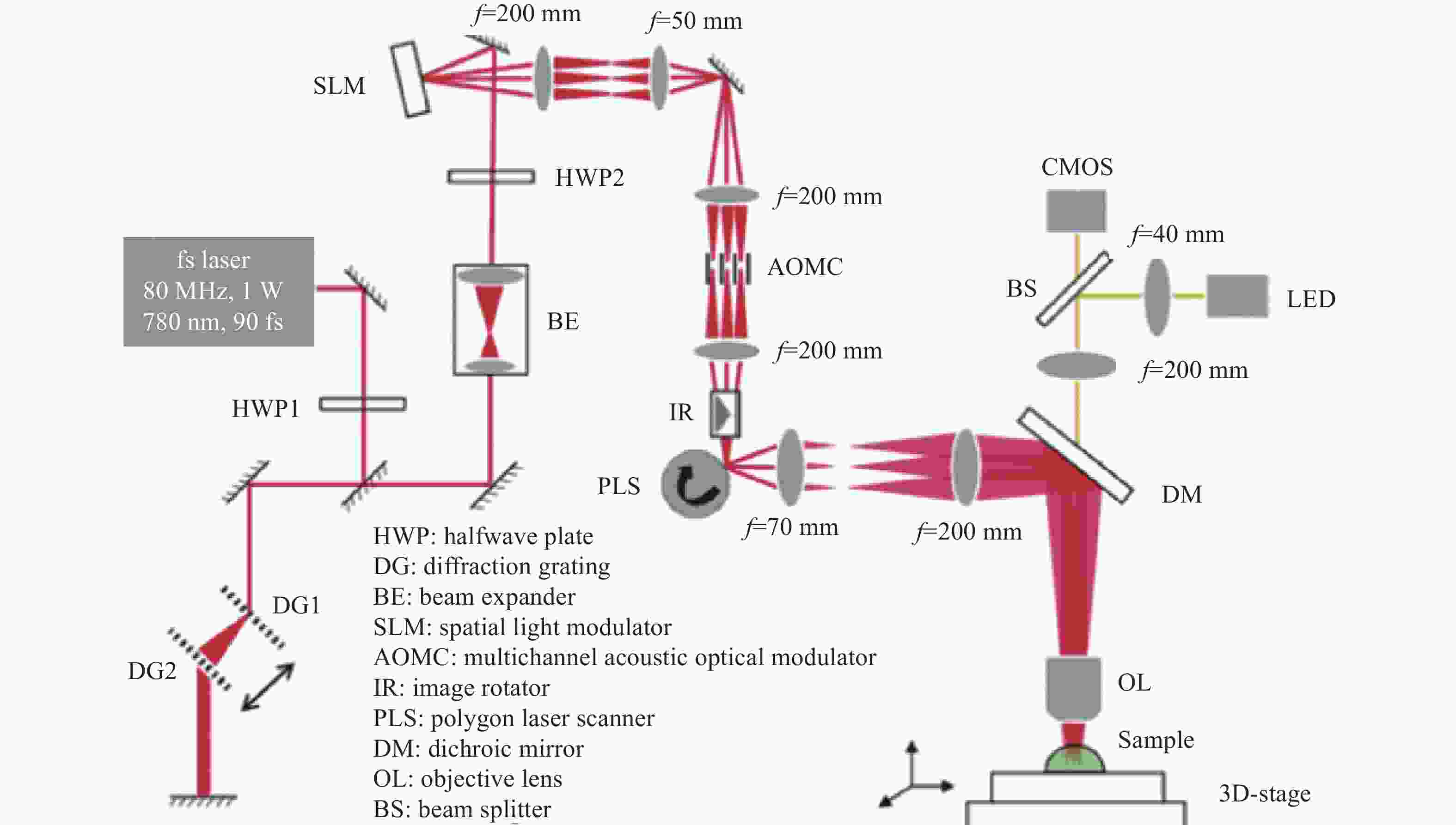
表 1 典型透明硬脆材料属性
Table 1. Typical transparent hard brittle material properties
Materials Melting temperature/K Boiling temperature/K Band gap/eV Moh's hardness Si[11] 1690 3540 1.10 7.0 SiC[12-14] 2970 3770 3.26 9.5 GaN[15] 1 973 2676 3.40 9.2 Fused silica[16-17] 1 986 3100 9.00 7.0 sapphire[18] 2350 3770 9.90 9.0 Diamond[19-20] 4750 5100 5.50 10 KDP[21-22] 451 653 5.91 2.5 YAG[23-24] 2220 2510 6.50 8.5 Lu2O3[25-26] 2760 4250 5.80 7.0 Y2O3[25, 27] 2690 4570 5.60 8.5  下载: 导出CSV
表 2 SiC晶锭激光切片设备主要参数
Table 2. Main parameters of SiC ingot laser slicing equipment
Shenzhen Han's Semiconductor Equipment Technology Co., Ltd[76] Westlake Instruments (Hangzhou) Technology Co., Ltd[78] Maximum cutting size SiC material, 8-inch downward compatible Processing dimensions SiC material, 4/6/8 in Ingot thickness - Ingot thickness ≤50 mm
(customizable)Maximum cutting thickness 5 mm Slice thickness 0.1-1.2 mm Cutting speed 400-1000 mm/s Slicing time ≤30 min
(6-inch continuous processing)Positioning accuracy ±1 μm Positioning accuracy <1 μm
下载: 导出CSV
-
[1] Uteza O, Bussi Re B, Canova F, et al. Laser-induced damage threshold of sapphire in nanosecond, picosecond and femtosecond regimes [J]. Applied Surface Science, 2007, 254(4): 799-803. doi: 10.1016/j.apsusc.2007.09.046 [2] Xie X, Zhou C, Wei X, et al. Laser machining of transparent brittle materials: from machining strategies to applications [J]. Opto-Electronic Advances, 2019, 2(1): 180017. doi: 10.29026/oea.2019.180017 [3] Liu M, Hu Y, Sun X, et al. Chemical etching mechanism and properties of microstructures in sapphire modified by femtosecond laser [J]. Applied Physics A, 2016, 123(1): 99. doi: 10.1007/s00339-016-0664-9 [4] 李佳群, 闫剑锋, 李欣, 等. 透明介质材料的超快激光微纳加工研究进展 [J]. 中国激光, 2021, 48(2): 0202019. doi: 10.3788/CJL202148.0202019 Li Jiaqun, Yan Jianfeng, Li Xi, et al. Research advancement on ultrafast laser microprocessing of transparent dielectrics [J]. Chinese Journal of Lasers, 2021, 48(2): 0202019. (in Chinese) doi: 10.3788/CJL202148.0202019 [5] Miyamoto I, Okamoto Y, Hansen A, et al. High speed, high strength microwelding of Si/Glass using ps-laser pulses [J]. Opt Express, 2015, 23(3): 3427-3439. doi: 10.1364/OE.23.003427 [6] Lee S A, Hwang J Y, Kim J P, et al. Dielectric characterization of transparent epitaxial Ga2O3 thin film on n-GaN∕Al2O3 prepared by pulsed laser deposition [J]. Applied Physics Letters, 2006, 89(18): 182906. doi: 10.1063/1.2374806 [7] Li Z, Wang X, Wang J, et al. Stealth dicing of sapphire sheets with low surface roughness, zero kerf width, debris/crack-free and zero taper using a femtosecond bessel beam [J]. Optics & Laser Technology, 2021, 135: 106713. doi: 10.1016/j.optlastec.2020.106713 [8] Liao K, Wang W, Mei X, et al. High quality full ablation cutting and stealth dicing of silica glass using picosecond laser bessel beam with burst mode [J]. Ceramics International, 2022, 48(7): 9805-9816. doi: 10.1016/j.ceramint.2021.12.182 [9] Lu Y, Li Y, Xie X, et al. Research advances of femtosecond laser-induced nanogratings for transparent materials [J]. Front Chem, 2022, 10: 1082651. doi: 10.3389/fchem.2022.1082651 [10] Han S, Yu H, He C, et al. Laser slicing of 4H-SiC wafers based on picosecond laser-induced micro-explosion via multiphoton processes [J]. Optics & Laser Technology, 2022, 154: 108323. doi: 10.1016/j.optlastec.2022.108323 [11] Morisaki H, Ping F W, Ono H, et al. Above-band-gap photoluminescence from Si fine particles with oxide shell [J]. Journal of Applied Physics, 1991, 70(3): 1869-1870. [12] Mohammed A F, Al-Jarwany Q A, Clarke A J, et al. Ablation threshold measurements and surface modifications of 193 nm laser irradiated 4H-SiC [J]. Chemical Physics Letters, 2018, 713: 194-202. doi: 10.1016/j.cplett.2018.09.057 [13] Weing Rtner R, Wellmann P J, Bickermann M, et al. Determination of charge carrier concentration in n- and p-doped SiC based on optical absorption measurements [J]. Applied Physics Letters, 2002, 80(1): 70-72. doi: 10.1063/1.1430262 [14] Yang B, Wang H, Peng S, et al. Precision layered stealth dicing of SiC wafers by ultrafast lasers [J]. Micromachines, 2022, 13(7): 1011. doi: 10.3390/mi13071011 [15] Andiwijayakusuma D, Saito M, Purqon A. Density functional theory study: Electronic structures of RE: GaN in wurtzite Gα15RE1N16 [J]. Journal of Physics: Conference Series, 2016, 739: 012027. doi: 10.7498/aps.65.133101 [16] Yang S T, Matthews M J, Elhadj S, et al. Thermal transport in CO2 laser irradiated fused silica: In situ measurements and analysis [J]. Journal of Applied Physics, 2009, 106(10): 103106. doi: 10.1063/1.3259419 [17] Heisterkamp A, Leyder S, Herman P R, et al. On the wavelength dependence of femtosecond laser interactions inside band gap solids [C]//Frontiers in Ultrafast Optics: Biomedical, Scientific, and Industrial Applications XIII, SPIE LASE, 2013, 8611: 861113. [18] Bufetova G A, Kashin V V, Rusanov S Y, et al. Determination of sapphire crystal melt refracttive index in visible range [J]. Journal of Crystal Growth, 2021, 575: 126355. doi: 10.1016/j.jcrysgro.2021.126355 [19] Kondrin M V, Lebed Y B, Brazhkin V V. Intrinsic planar defects in diamond and the upper limit on its melting temperature [J]. Diamond and Related Materials, 2020, 110: 108114. [20] Cao Z, Aslam D. Fabrication technology for single-material MEMS using polycrystalline diamond [J]. Diamond and Related Materials, 2010, 19(10): 1263-1272. doi: 10.1016/j.diamond.2010.06.005 [21] Boysen D A, Haile S M, Liu H, et al. Conductivity of potassium and rubidium dihydrogen phosphates at high temperature and pressure [J]. Chemistry of Materials, 2004, 16(4): 693-697. doi: 10.1021/cm034954a [22] 侯碧辉, 王雅丽, 常新安, 等. KH2PO4晶体的太赫兹-紫外光谱 [J]. 光谱学与光谱分析, 2010, 30: 2881-2884. doi:10.3964/j.issn.1000-0593(2010)11-2881-04 Hou Bihui, Wang Yali, Chang Xinan, et al. THz-ultraviolet spectra of KDP crystal [J]. Spectroscopy and Spectral Analysis, 2010, 30(11): 2881-2884. (in Chinese) doi: 10.3964/j.issn.1000-0593(2010)-11-2881-04 [23] Kumar A, Kumar R, Verma N, et al. Effect of the band gap and the defect states present within band gap on the non-linear optical absorption behaviour of yttrium aluminium iron garnets [J]. Optical Materials, 2020, 108: 110163. doi: 10.1016/j.optmat.2020.110163 [24] 丰盛, 单志涛, 潘瑞琨, 等. 基于气动悬浮激光加热技术 YAG 熔体高温热物理性能评测 [J]. 无机材料学报, 2018, 33(12): 1297-1302. doi:10.3788/CJL202148.0202019 Feng Sheng, Shan Zhitao, Pan Ruikun, et al. Thermo-physical property of YAG melt measured by aerodynamic levitation technique [J]. Journal of Inorganic Materials, 2018, 33(12): 1297-1302. (in Chinese) doi: 10.15541/jim20180104 [25] Pavlik A, Ushakov S V, Navrotsky A, et al. Structure and thermal expansion of Lu2O3 and Yb2O3 up to the melting points [J]. Journal of Nuclear Materials, 2017, 495: 385-391. doi: 10.1016/j.jnucmat.2017.08.031 [26] Seguini G, Bonera E, Spiga S, et al. Energy-band diagram of metal/Lu2O3/silicon structures [J]. Applied Physics Letters, 2004, 85(22): 5316-5318. [27] Wang W C, Badylevich M, Afanas’ev V V, et al. Band alignment and electron traps in Y2O3 layers on (100)Si [J]. Applied Physics Letters, 2009, 95(13): 132903. doi: 10.1063/1.3236536 [28] 栾美玲, 郑家鑫, 孙相超, 等. 液体辅助激光加工硬脆材料及其应用[J]. 光电工程, 2023, 50(03): 61-78. doi: 10.12086/oee.2023.220328 Luan Meiling, Zheng Jiaxin, Sun Xiangchao, et al. Liquid-assisted laser fabrication of hard materials and applications [J]. Opto-Electronic Engineering, 2023, 50(3): 61-78. (in Chinese) doi: 10.12086/oee.2023.220328 [29] Srinivasasn R, Sutcliffe E, Braren B. Ablation and etching of polymethylmethacrylate by very short (160 fs) ultraviolet (308 nm) laser pulses [J]. Applied Physics Letters, 1987, 51(16): 1285-1287. doi: 10.1063/1.99001 [30] Cheng C W, Tsai X Z, Chen J S. Micromachining of stainless steel with controllable ablation depth using femtosecond laser pulses [J]. The International Journal of Advanced Manufacturing Technology, 2016, 85(9): 1947-1954. doi: 10.1007/s00170-016-8821-z [31] Hunsche S, Leo K, Kurz H, et al. Exciton absorption saturation by phase-space filling: Influence of carrier temperature and density [J]. Phys Rev B Condens Matter, 1994, 49(23): 16565-16568. doi: 10.1103/physrevb.49.16565 [32] Fang Z, Chen J, Jiang X, et al. Repair of fused silica damage using selective femtosecond laser-induced etching [J]. Crystals, 2023, 13(2): 309. doi: 10.3390/cryst13020309 [33] Grigogrev F V, Sulimov V B, Tikhonravov A V. Laser-induced thermal stresses in dense and porous silicon dioxide films [J]. Coatings, 2021, 11(4): 394. doi: 10.3390/coatings11040394 [34] Polynkin P. Intense femtosecond shaped laser beams for writing extended structures inside transparent dielectrics [J]. Applied Physics A, 2013, 114(1): 143-149. doi: 10.1007/s00339-013-8133-1 [35] Zheltikov A M. Ultrafast optical switching of an ionized medium by interfering ultrashort laser pulses [J]. JETP Letters, 2009, 90(2): 90-95. doi: 10.1134/s0021364009140021 [36] Hu K, Guo Z, Cao T, et al. Study on the polarization dependence of nonlinear absorption of ultrafast laser pulses in bulk fused silica [J]. Opt Express, 2022, 30(6): 8949-8958. doi: 10.1364/OE.449608 [37] Wu S, Wu D, Xu J, et al. Characterization and mechanism of glass microwelding by double-pulse ultrafast laser irradiation [J]. Optics Express, 2012, 20(27): 28893-28905. doi: 10.1364/OE.20.028893 [38] Bogatskaya A, Gulina Y, Smirnov N, et al. An experimental study of multiphoton ionization in fused silica at IR and visible wavelengths [J]. Photonics, 2023, 10(5): 515. doi: 10.3390/photonics10050515 [39] Koz K M, Troj N F, Mal P. Hot-carrier transport in diamond controlled by femtosecond laser pulses [J]. New Journal of Physics, 2015, 17(5): 053027. doi: 10.1088/1367-2630/17/5/053027 [40] Marks M R, Cheong K Y, Hassan Z. A review of laser ablation and dicing of Si wafers [J]. Precision Engineering, 2022, 73: 377-408. doi: 10.1016/j.precisioneng.2021.10.001 [41] Ponader C W, Schroeder J F, Sterltsov A M. Origin of the refractive-index increase in laser-written waveguides in glasses [J]. Journal of Applied Physics, 2008, 103(6): 063516. doi: 10.1063/1.2888561 [42] Miura K, Qiu J, Inouye H, et al. Photowritten optical waveguides in various glasses with ultrashort pulse laser [J]. Applied Physics Letters, 1997, 71(23): 3329-3331. doi: 10.1063/1.120327 [43] Efimov O M, Glebov L B, Richardson K A, et al. Waveguide writing in chalcogenide glasses by a train of femtosecond laser pulses [J]. Optical Materials, 2001, 17(3): 379-386. doi: 10.1016/s0925-3467(01)00062-3 [44] Bain F M, Silva W F, Lagatskya A, et al. Microspectroscopy of ultrafast laser inscribed channel waveguides in Yb: tungstate crystals [J]. Applied Physics Letters, 2011, 98(14): 141108. doi: 10.1063/1.3573999 [45] Sudrie L, Franco M, Prade B, et al. Writing of permanent birefringent microlayers in bulk fused silica with femtosecond laser pulses [J]. Optics Communications, 1999, 171(4): 279-284. doi: 10.1016/s0030-4018(99)00562-3 [46] Liang F, Vallee R, Chin S L. Mechanism of nanograting formation on the surface of fused silica [J]. Opt Express, 2012, 20(4): 4389-4396. doi: 10.1364/OE.20.004389 [47] Taylor R, Hnatovsky C, Simove E. Applications of femtosecond laser induced self-organized planar nanocracks inside fused silica glass [J]. Laser & Photonics Review, 2008, 2(1): 26-46. doi: 10.1002/lpor.200710031 [48] Richter S, Heinrich M, D Ring S, et al. Nanogratings in fused silica: Formation, control, and applications [J]. Journal of Laser Applications, 2012, 24(4): 042008. doi: 10.2351/1.4718561 [49] Cheng W, Wang Z, Liu X, et al. Microexplosions in bulk sapphire driven by simultaneously spatially and temporally focused femtosecond laser beams [J]. Opt Lett, 2023, 48(3): 751-754. doi: 10.1364/OL.482320 [50] 彭娜娜, 霍燕燕, 周侃, 等. 飞秒激光诱导自组织纳米周期结构及其光学特性的研究进展[J]. 物理学报, 2013, 62(9): 9-16. doi: 10.7498/aps.62.094201 Peng Nana, Huo Yanyan, Zhou Kan, et al. The development of femtosecond laser-induced periodic nanostructures and their optical properties [J]. Acta Physica Sinica, 2013, 62(9): 9-16. (in Chinese) doi: 10.7498/aps.62.094201 [51] 卢轶明, 高炳荣, 刘学青, 等. 飞秒激光制备耐高温蓝宝石内部几何相位波带片(特邀)[J]. 光子学报, 2021, 50(6): 0650107. doi: 10.3788/gzxb20215006.0650107 Lu Yiming, Gao Bingrong, Liu Xueqing, et al. Fabrication of high temperature resistant geometric phase element inside sapphire by femtosecond laser (Invited) [J]. Acta Photonica Sinica, 2021, 50(6): 0650107. (in Chinese) doi: 10.3788/gzxb20215006.0650107 [52] Shimotsuma Y, Kazansky P G, Qiu J, et al. Self-organized nanogratings in glass irradiated by ultrashort light pulses [J]. Phys Rev Lett, 2003, 91(24): 247405. doi: 10.1103/PhysRevLett.91.247405 [53] Juodkazis S, Nishimura K, Tanaka S, et al. Laser-induced microexplosion confined in the bulk of a sapphire crystal: Evidence of multimegabar pressures [J]. Physical Review Letters, 2006, 96(16): 166101. doi: 10.1103/PhysRevLett.96.166101 [54] Huang Y, Wu X, Liu H, et al. Fabrication of through-wafer 3D microfluidics in silicon carbide using femtosecond laser [J]. Journal of Micromechanics and Microengineering, 2017, 27(6): 065005. doi: 10.1088/1361-6439/aa68cb [55] Wang J, Fang F, An H, et al. Laser machining fundamentals: micro, nano, atomic and close-to-atomic scales [J]. International Journal of Extreme Manufacturing, 2023, 5(1): 012005. doi: 10.1088/2631-7990/acb134 [56] Zhai Z, Wang W, Zhao J, et al. Influence of surface morphology on processing of C/SiC composites via femtosecond laser [J]. Composites Part A: Applied Science and Manufacturing, 2017, 102: 117-125. doi: 10.1016/j.compositesa.2017.07.031 [57] Ohmura E. Temperature Rise of Silicon due to Absorption of Permeable Pulse Laser [M]//Heat Transfer-Engineering Applications. London: IntechOpen, 2011. [58] Paoagiakoumou E, Ronzitti E, Emiliani V. Scanless two-photon excitation with temporal focusing [J]. Nat Methods, 2020, 17(6): 571-581. doi: 10.1038/s41592-020-0795-y [59] Salter P S, Booth M J. Adaptive optics in laser processing [J]. Light Sci Appl, 2019, 8: 110. doi: 10.1038/s41377-019-0215-1 [60] Salter P S, Baum M, Alexeev I, et al. Exploring the depth range for three-dimensional laser machining with aberration correction [J]. Opt Express, 2014, 22(15): 17644-17656. doi: 10.1364/OE.22.017644 [61] Kim E, Shimotsuma Y, Sakakura M, et al. 4H-SiC wafer slicing by using femtosecond laser double-pulses [J]. Optical Materials Express, 2017, 7(7): 2450. doi: 10.1364/ome.7.002450 [62] Jia X, Chen Y, Liu L, et al. Combined pulse laser: Reliable tool for high-quality, high-efficiency material processing [J]. Optics & Laser Technology, 2022, 153: 108209. doi: 10.1016/j.optlastec.2022.108209 [63] Hernandez-rueda J, Siegel J, Puerto D, et al. Ad-hoc design of temporally shaped fs laser pulses based on plasma dynamics for deep ablation in fused silica [J]. Applied Physics A, 2012, 112(1): 185-189. doi: 10.1007/s00339-012-7238-2 [64] Rosenfeld A, Rohloff M, H Hm S, et al. Formation of laser-induced periodic surface structures on fused silica upon multiple parallel polarized double-femtosecond-laser-pulse irradiation sequences [J]. Applied Surface Science, 2012, 258(23): 9233-9236. doi: 10.1016/j.apsusc.2011.09.076 [65] 刘文凤, 孙明营, 石逸群, 等. 时域整形皮秒激光双脉冲烧蚀玻璃表面特性[J]. 中国激光, 2023, 50(12): 1202201. doi: 10.3788/CJL221235 Liu Wenfeng, Sun Mingying, Shi Yiqun, et al. Picosecond laser ablation of glass surface by dual-pulse temporal [J]. Chinese Journal of Lasers, 2023, 50(12): 1202201. (in Chinese) doi: 10.3788/CJL221235 [66] 王洪庆, 温积森, 杨臻垚, 等. 高速并行双光子激光直写光刻系统[J]. 中国激光, 2022, 49(22): 121-128. doi: 10.3788/CJL202249.2202009 Wang Hongqing, Wen Jisen, Yang Zhenyao, et al. High-speed parallel two-photon laser direct writing lithography system [J]. Chinese Journal of Lasers, 2022, 49(22): 2202009. (in Chinese) doi: 10.3788/CJL202249.2202009 [67] Cao X W, Lu Y M, Fan H, et al. Wet-etching-assisted femtosecond laser holographic processing of a sapphire concave microlens array [J]. Appl Opt, 2018, 57(32): 9604-9608. doi: 10.1364/AO.57.009604 [68] Sanchez E K, Ha S, Grim J, et al. Assessment of polishing-related surface damage in silicon carbide [J]. Journal of the Electrochemical Society, 2002, 149(2): G131. doi: 10.1149/1.1430416 [69] Grim J R, Benamara M, Skowronski M, et al. Transmission electron microscopy analysis of mechanical polishing-related damage in silicon carbide wafers [J]. Semiconductor Science and Technology, 2006, 21(12): 1709-1713. doi: 10.1088/0268-1242/21/12/035 [70] Shi Erwei. The Growth and Defects of Silicon Carbide Crystal [M]. Beijing: Science Press, 2012. (in Chinese) [71] Swoboda M, Beyer C, Rieske R, et al. Laser assisted SiC wafering using cold split [J]. Materials Science Forum, 2017, 897: 403-406. doi: 10.4028/www.scientific.net/MSF.897.403 [72] Kling R, Washio K, Klotzbach U, et al. New laser slicing technology named KABRA process enables high speed and high efficiency SiC slicing [Z]. Laser-based Micro- and Nanoprocessing XII, 2018. [73] Wang H, Chen Q, Yao Y, et al. Influence of surface preprocessing on 4H-SiC wafer slicing by using ultrafast laser [J]. Crystals, 2022, 13(1): 15. doi: 10.3390/cryst13010015 [74] Zhang Y, Xie X, Huang Y, et al. Internal modified structure of silicon carbide prepared by ultrafast laser for wafer slicing [J]. Ceramics International, 2023, 49(3): 5249-5260. doi: 10.1016/j.ceramint.2022.10.043 [75] Geng W, Shao Q, Pei Y, et al. Slicing of 4H-SiC wafers combining ultrafast laser irradiation and bandgap-selective photo-electrochemical exfoliation [J]. Advanced Materials Interfaces, 2023, 10(21): 202300200. doi: 10.1002/admi.202300200 [76] HSET. SiC晶锭激光切片设备 [EB/OL]. (2022-01-02) [2023-10-19]. https://www.szhset.com/productdetail/62.html. [77] Delphi Laser. Laser processing equipment for silicon carbide wafers [EB/OL]. (2023-07-10) [2023-10-19]. http://www.delphilaser.com/?content/319. [78] Westlake Instruments. SiC substrate laser peeling equipment [EB/OL]. (2023-05-24) [2023-10-19]. http://www.westlakeinst.com/products/61.html. [79] Disco. Development of a KABRA® Process Optimized for the Production of GaN Wafers [EB/OL]. (2021-10-01) [2023-10-19]. https://www.disco.co.jp/eg/news/corp/kabra_gan.html. [80] Voronenkov V, Bochkareva N, Gorbunov R, et al. Laser slicing: A thin film lift-off method for GaN-on-GaN technology [J]. Results in Physics, 2019, 13: 102233. doi: 10.1016/j.rinp.2019.102233 [81] Kaule F, Swoboda M, Beyer C, et al. Laser-assisted spalling of large-area semiconductor and solid state substrates [J]. MRS Communications, 2018, 8(1): 127-131. doi: 10.1557/mrc.2017.136 [82] Dross F, Robbelein J, Vandevelde B, et al. Stress-induced large-area lift-off of crystalline Si films [J]. Applied Physics A, 2007, 89(1): 149-152. doi: 10.1007/s00339-007-4195-2 [83] Hirai H, Hidai H, Matsusaka S, et al. Diamond slicing using ultrashort laser-induced graphitization and additional nanosecond laser illumination [J]. Diamond and Related Materials, 2019, 96: 126-133. doi: 10.1016/j.diamond.2019.04.037 [84] Kiel F, Bulgakova N M, Ostendorf A, et al. Selective delamination upon femtosecond laser ablation of ceramic surfaces [J]. Physical Review Applied, 2019, 11(2): 024038. doi: 10.1103/PhysRevApplied.11.024038 -

 点击查看大图
图(13) / 表(2)
计量
- 文章访问数: 176
- HTML全文浏览量: 62
- PDF下载量: 60
- 被引次数: 0

