


-
超快辐射指的是时间低于100 ps、涉及X射线至远红外波段的宽光谱范围以及α粒子、质子、中子等粒子的快速信号发射过程。通过对这些粒子或光波的研究可以有效还原和评估超快辐射过程,因此研究者们在这些光子、粒子超快现象的快响应探测器上进行了许多工作[1-3]。作为核爆γ射线辐射探测系统的核心部件,光电阴极的响应时间必须小于超快探测系统的时间分辨要求,且其发射的电子束必须具备尽可能小的横向扩散和尽可能小的纵向尺寸[4]。在各种光电阴极材料中,GaAs具有阈值波长可调、暗发射小、发射电子能量分布集中等优点,且相比于金属、碱-锑等光电阴极材料,GaAs具有更小的发射度,因此其在超快探测、窄脉冲激光等应用方面具备明显优势[5-8]。为了进一步提升GaAs光电阴极的时间分辨特性,研究者通过在GaAs材料内部构建内建电场的方式形成了梯度掺杂光电阴极[9]和指数掺杂光电阴极[6],通过给光电阴极添加外加电场的方式形成了场助光电阴极[10],加快了光电子在材料内部的传输速率,并设计了多种光电阴极结构,将GaAs光电阴极的响应时间提升至10 ps左右。然而这些结构的实现对光电阴极材料的外延工艺和器件的制备工艺提出了较高的要求,目前国内外还无法大规模量产变掺杂和场助光电阴极。还有研究者指出,通过将GaAs光电阴极的负电子亲和势调整为一个较小的正电子亲和势可以使得GaAs光电阴极的响应时间达到1 ps,但是这种方式会使得GaAs光电阴极的量子效率产生较大的衰减[11-12]。传统GaAs光电阴极具备较高的量子效率和成熟稳定的制备工艺,因此,文中在传统GaAs光电阴极的基础上研究后界面复合速率、电子扩散系数、激活层厚度对其时间响应特性的影响,为GaAs光电阴极的结构设计和材料参数设计提供理论依据,同时为快响应GaAs光电阴极的实验研究和应用提供必要的理论指导。
-
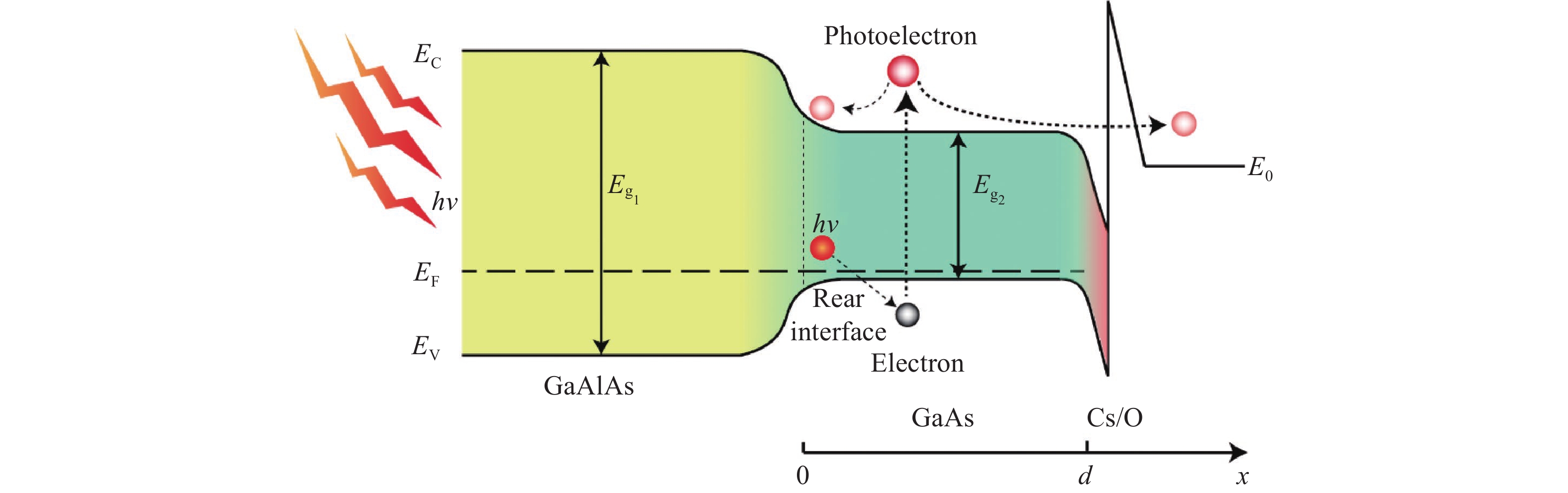
图1为传统透射式GaAs光电阴极的能带图。根据Spicer光电发射“三步模型”理论,首先,光照下能量小于GaAlAs的禁带宽度而大于GaAs禁带宽度的光子被p-GaAs吸收而激发产生光生电子。其次,绝大多数光电子被激发到导带后处于能量较高的热电子状态,之后将通过散射同时向GaAlAs/GaAs界面和GaAs发射层表面(x=d)作扩散运动。最后,到达光电阴极表面的光电子隧穿表面势垒发射到真空中。影响GaAs光电阴极时间响应特性的主要因素为Spicer光电发射模型中第二步的电子扩散迁移行为。光电子通过扩散迁移在光电阴极体内的分布是时间的函数,通过矩阵差分求解GaAs激活层内光电子的连续性方程(公式(1))和一系列边界条件(公式(2)~(4)),可以求得GaAs光电阴极出射光电子流密度方程(公式(5))的数值解曲线,曲线的半峰宽即为透射式GaAlAs/GaAs光电阴极的响应时间。
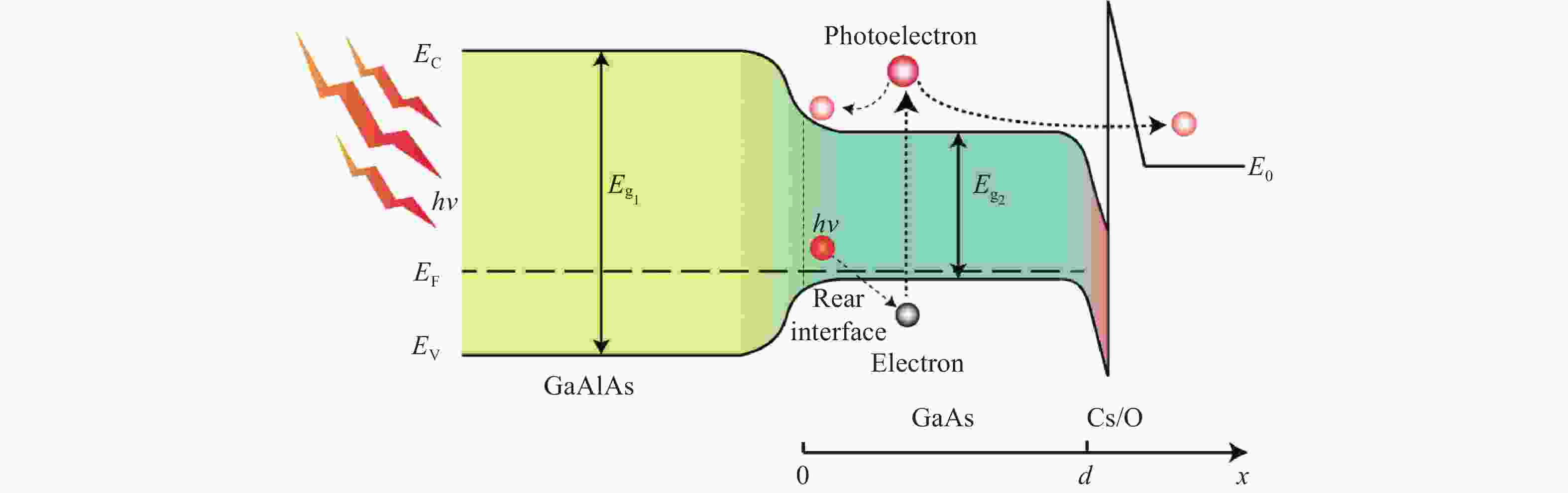
Figure 1. Energy band diagram of traditional transmission-mode GaAs photocathode
式中:Δ
n为光生电子的分布;t为时间;Dn为光电子在GaAs界面的扩散系数;x为距离GaAlAs/GaAs界面的距离;τn为光电子在GaAs中的寿命;s为GaAlAs/GaAs界面的复合速率;d为GaAs激活层厚度;F为与GaAs吸收系数α相关的值: 式中:R为GaAs光电阴极光照面的反射率;η为光生载流子的产生率;N为入射光子数;A为光阴极面积;α为GaAs的吸收系数;Δt为光源的脉冲宽度。
-
从物理模型可以得出,对响应时间造成影响的主要物理参数包括GaAs激活层厚度d、GaAs电子扩散系数Dn和GaAs/GaAlAs界面的后界面复合速率Sv,现对这三种因素对GaAs光电阴极时间响应特性的影响进行系统的理论计算。目前传统GaAs光电阴极的电子扩散系数Dn=50 cm2/s,GaAs/GaAlAs界面的后界面复合速率Sv=105 cm/s,激活层厚度d=1.5 μm,在对其中一个参数进行计算分析时,另外两个参数保持上述值不变。研究中所采用的入射光波长为530 nm。
-
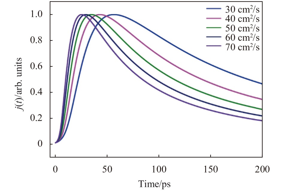
图2为不同电子扩散系数下GaAs光电阴极出射光电子流密度随时间的变化曲线。从图中可以明显看出,随GaAs电子扩散系数的增大,GaAs光电阴极响应速率不断加快。电子扩散系数是单位浓度梯度作用下的粒子流密度,可用于表征电子在材料内部浓度梯度下的运动速率,电子扩散系数越大,电子运动速率越快,且电子扩散系数与电子迁移率之间存在Einstein正比关系。因此,随着电子扩散系数的增大,电子迁移率也增大,从而使得响应速率不断加快。

Figure 2. Curve of the photoelectron current density with time in GaAs photocathode with different electron diffusion coefficients
表1为GaAs光电阴极响应时间与GaAs电子扩散系数的对应关系表。可以看出,随着电子扩散的不断增大,响应速率增长的速度不断变慢,当电子扩散系数增大到70 cm2/s后,响应速率基本达到饱和,不再随电子扩散系数的增大而增大。这主要是因为电子扩散系数不断增大,电子迁移速率不断加快,在GaAs这种双能谷半导体内,这些高能电子将向有效质量较大的次能谷中跃迁,此时将出现负电阻导致电子迁移率下降。同时,次能谷中的高能电子将与声子发生散射而损失能量,因而使得电子迁移速率达到饱和。
Item Value Dn/cm2·s−1 30 40 50 60 70 ΔT/ps 329 249 203 170 148 Table 1. Correspondence table of GaAs photocathode response time and electron diffusion coefficient
-
GaAs/GaAlAs后界面复合速率指的是GaAs/GaAlAs界面处单位表面积电子-空穴对的复合数,图3为不同后界面复合速率下GaAs光电阴极出射光电子流密度随时间的变化曲线。从图中可以看出,GaAs光电阴极的响应速率随后界面复合速率的增大而加快。产生这种现象的原因在于界面复合中心浓度的增大导致更多的电子向复合中心补充,阴极内部局部电子聚集区域增多,一方面所形成的电势对电子的扩散迁移运动有一定的加速效果,另一方面所形成的局域电场会对GaAs/GaAlAs界面的能带结构会产生一定的影响,导致界面势垒的降低从而引起GaAs内部电子流密度的增大[13],因此使得GaAs光电阴极的响应速率加快。
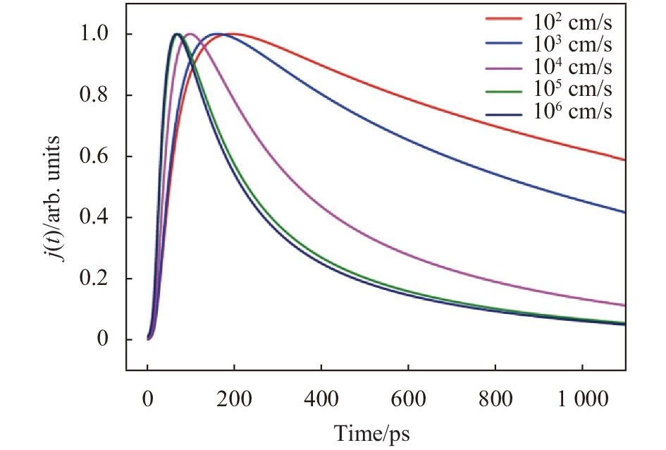
Figure 3. Curve of the photoelectron current density with time in GaAs photocathode with different rear interface recombination rate
表2为GaAs光电阴极响应时间与GaAs/GaAlAs后界面复合速率的对应关系表。可以看出,在后界面复合速率较小时,其对响应时间的影响较大,随后界面复合速率的增大响应速率快速增大。当其增大到约为106 cm/s时,响应速率达到饱和,不再随后界面复合速率的增大而增大。出现这种现象可能的原因为当后界面复合速率增大到一定值后,光电子的运动速率也增长到一个较大值,因此光电子具备较大的能量而发生能谷跃迁,出现负电阻和声子散射导致电子能量下降,最终电子运动速率达到稳定饱和。
Item Value Sv/cm·s−1 102 103 104 105 106 ΔT/ps 1354 845 313 203 191 Table 2. Correspondence table of GaAs photocathode response time and rear interface recombination rate
-
图4为不同激活层厚度下GaAs光电阴极出射光电子流密度随时间的变化曲线图,图中对GaAs光电阴极的出射光电子流密度进行了归一化处理。从图中可以明显看出,随着激活层厚度的降低,GaAs光电阴极的响应时间迅速减小,这主要是激活层厚度减小使得电子在向真空发射前在激活层内所需扩散迁移的距离变短,从而电子在阴极内部的扩散迁移时间变短,使得光电阴极的响应速率加快。
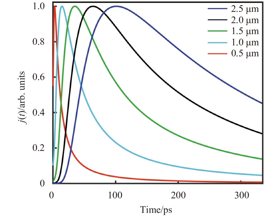
Figure 4. Curve of the photoelectron current density with time in GaAs photocathode with different active layer thickness
表3为GaAs光电阴极响应时间与激活层厚度的对应关系表。可以看出,激活层厚度从2.5 μm降低到0.5 μm,响应时间从533 ps缩短至23 ps,响应速率提升了22倍,可以满足大部分光子、粒子辐射探测系统的快响应需求。
Item Value d/μm 2.5 2.0 1.5 1.0 0.5 ΔT/ps 533 360 203 90 23 Table 3. Correspondence table of GaAs photocathode response time and active layer thickness
-
文中通过对光电子扩散模型的计算,较为系统地研究了电子扩散系数、激活层厚度及后界面复合速率对GaAs光电阴极时间分辨特性的影响。研究结果表明,以上三种物理因素对GaAs光电阴极的响应速率均有较大影响。当电子扩散系数和后界面复合速率增大到一定值后,GaAs光电阴极会产生最大饱和响应速率。激活层厚度对响应时间的影响最大,通过优化激活层厚度可以使GaAs光电阴极的响应时间缩短至20 ps左右,可满足大多数光子、粒子对探测系统光电阴极的时间分辨要求。文中的研究结果为进一步优化光电阴极的结构和材料参数提供了一定的理论依据,为快响应GaAs光电阴极的实验设计与应用提供了必要的理论支撑。
Study on the time-resolved characteristics of the transmission-mode GaAs photocathode
doi: 10.3788/IRLA20210761
- Received Date: 2021-10-18
- Rev Recd Date: 2022-01-09
- Publish Date: 2022-08-31
Fund Project:
National Natural Science Foundation of China (61771245);National Defense Basic Scientific Research Program(JCKY2018208 B016)
-
Key words:
- response time /
- GaAs photocathode /
- photoelectron diffusion model
Abstract: Time-resolved characteristics are a very important performance parameter of GaAs photocathodes used in pump detection and other fields. In this paper, the photoelectron continuity equation and the outgoing photoelectron flow density equation are calculated by solving the photoelectron diffusion model by the matrix difference method. The factors affecting the time-resolved characteristics of the GaAs photocathode include the recombination rate of the GaAs/GaAlAs rear interface, GaAs electron diffusion coefficient and GaAs active layer thickness. Then, the effects of these three physical factors on the time-resolved characteristics of the GaAs photocathode are systematically studied. The research results show that the GaAs electron diffusion coefficient and the GaAs/GaAlAs rear interface recombination rate have a nonlinear proportional relationship with the response rate of the photocathode, and the saturation response rate of the GaAs photocathode will appear as the two increase. The thickness of the GaAs active layer has the greatest impact on the response time of the GaAs photocathode. The response time of the GaAs photocathode can be reduced to 20 ps by appropriately thinning the thickness of the active layer, which can meet the fast response requirements for most photon and particle detection. This study provides necessary theoretical support for the experiment and application of a fast-response GaAs photocathode.


 DownLoad: