

-
随着科技的飞速发展,光学显微系统已越来越广泛地应用于人们的生活之中,如电子学、医学、生物学等领域[1-3]。但由于显微系统的分辨率要求较高,系统片数通常较多,对装调要求苛刻。为呈现更好的图像质量,研究人员从不同角度出发来解决此问题:2015年中国科学院长春光学精密机械与物理研究所设计了一款20×平场复消色差显微物镜[4];2016年研究人员将光学设计过程中的优化函数与图像处理算法的约束条件结合在一起,获得高分辨率图像[5];2018年中国科学院长春光学精密机械与物理研究所又设计出了一款基于液体透镜自动聚焦的显微成像系统,消除离焦影响 [6];2019年无透镜成像技术也正在兴起[7]。
显微光学系统中存在着像质设计优化与装调难度之间的固有矛盾,在设计优化阶段为了提升像质,尽可能地采用更多的光学元件以及特殊光学元件来达到设计目的,同时带来了每个元件单独承担的像差系数大幅提升,此时对于装调提出了更大的挑战,甚至有些装调要求现有手段无法实现,导致设计结果成为无效设计。笔者更希望能存在一个合理的系统,使其在成像质量较好的同时具有较宽松的装配要求,并且具有工艺可重复性。
波像差的大小可以直接用于评价系统的成像质量,也可以用每个元件所承担的波像差贡献进行单个元件的公差敏感度评估分析。在包含多个元件的光学系统设计中,各元件表面的波像差是可以叠加的,即整个系统出瞳位置的波像差等于每个元件表面波像差之和。所以,减小各元件表面的初级像差值可以有效降低系统的公差灵敏度[8]。因此文中提出用小像差互补设计的方法对光学系统进行优化设计。
以一红外显微光学系统为例,对比传统系统设计方法与小像差互补设计法的设计结果,表明在满足成像质量要求的前提下,基于小像差互补设计方法设计的系统中各个元件表面初级像差系数明显减小,更易于实际加工与装调。
-
光学系统的最终实际成像质量不仅受到系统自身像差校正情况的影响,还受到元件加工和系统装调水平的制约,初级像差系数即赛德尔系数表征了各元件表面的初级像差,当初级像差较大时,说明此面较为敏感,对于加工和装调会产生一定的影响,并且赛德尔系数和波像差系数具有特定的正比关系[8]。因此,笔者在波像差理论基础上提出了一种小像差互补的设计方法。小像差互补设计方法将各个元件波像差最小的表达式嵌入到优化软件中,寻找出一个使各元件表面的初级像差系数均较小的解决方案,可以改善像差系数的分布并提高系统容差,进而减小加工和装调难度。
针对折射球面和非球面这两种常见面型,分别对其波像差表达式进行了推导。以折射球面为例,由于总的波像差系数等于各个像差波像差系数的和[8],因此其波像差公式可表示为:
$$W\left( {r,\theta ,{h'}} \right) = {W_{040}} + {W_{131}} + {W_{222}} + {W_{220}} + {W_{311}}$$ (1) 其中,各个像差的波像差系数表达式[8]为:
$${W_{040}}{\rm{ = }}{a_{ss}}{r^4}$$ (2) $${W_{131}} = {a_{cs}}{h'}{r^3}\cos \theta $$ (3) $${W_{222}} = {a_{as}}{h'^{2}}{r^2}{\cos ^2}\theta $$ (4) $${W_{220}} = {a_{ds}}{h'^{2}}{r^2}$$ (5) $${W_{311}} = {a_{ts}}{h'^{3}}r\cos \theta $$ (6) 则光阑在任意位置时折射球面的波像差公式如下:
$$\begin{split} W\left( {r,\theta ,{h'}} \right) =& {a_{ss}}{r^4} + {a_{cs}}{h'}{r^3}\cos \theta + {a_{as}}{h^{'2}}{r^2}{\cos ^2}\theta + \\ & {a_{ds}}{h^{'2}}{r^2} + {a_{ts}}{h^{'3}}r\cos \theta \end{split}$$ (7) 同样地,光阑在任意位置时折射二次圆锥非球面的波像差公式如下:
$$\begin{split} W\left( {r,\theta ,{h'}} \right) =& {a_{sc}}{r^4} + {a_{cc}}{h'}{r^3}\cos \theta + {a_{ac}}{h^{'2}}{r^2}{\cos ^2}\theta + \\ & {a_{dc}}{h^{'2}}{r^2} + {a_{tc}}{h^{'3}}r\cos \theta \end{split} $$ (8) 式中:r,θ对应于出瞳上任意点Q的极坐标(r, θ),如图1所示;h'为像高,各波像差系数符号如表1所示。

图 1 出瞳上任意点Q的极坐标
Figure 1. Polar coordinates of a point Q at the exit pupil
表 1 两种面型五种单色像差的波像差系数
Table 1. Coefficients in five kinds of monochromatic aberrations on two surfaces
Spherical
aberrationComa Astigmatism Field
curvatureDistortion Refractive
sphere surfaceass acs aas ads ats Refractive
conic surfaceasc acc aac adc atc -
由于总的波像差系数等于各个像差波像差系数的和,令最终系统的波像差趋于零,建立相应的数学模型,使每个表面的波像差系数接近极小值。具体模型如下:
$${W_{040}}\left( {1,2,3 \cdot \cdot \cdot i} \right) \to 0$$ …
$${W_{311}}\left( {1,2,3 \cdot \cdot \cdot i} \right) \to 0$$ $${W_{040}}\left( 1 \right) + {W_{040}}\left( 2 \right) + {W_{040}}\left( 3 \right) + \cdot \cdot \cdot + {W_{040}}\left( i \right) \to 0$$ …
$$ {W_{311}}\left( 1 \right) + {W_{311}}\left( 2 \right) + {W_{311}}\left( 3 \right) + \cdot \cdot \cdot + {W_{311}}\left( i \right) \to 0 $$ 式中:W040(i)、W131(i)、W222(i)、W220(i)、W311(i)分别表示第i个面上的球差、彗差、像散、场曲及畸变的波像差系数。
基于小像差互补设计方法的数学模型编写相应的ZPL宏,用于软件精确控制优化设计目标函数。在此展示宏的一部分。以优化彗差为例:
as=(1/8)*n1*n1*(1/R−1/S1)*(1/R−1/S1)*(1/(n1*S1)−1/(n0*S))
ass=POWR((S1/L),4)*as
acs= 4*d *ass
acc=4*(d*ass-sg*g*POWR((S1/L),3))
if(mode==1)
COMA=acs*h1*POWR(r1,3)
endif
if(mode==2)
COMA=acc*h1*POWR(r1,3)
endif
W131=COMA/WAVL(wave)*1000
-
以一红外显微光学系统为例对小像差互补设计方法进行验证,设计参数如表2所示。
表 2 红外显微光学系统的设计参数
Table 2. Parameters of infrared microscope system
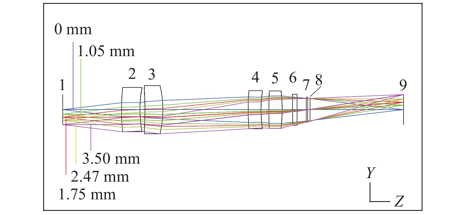
Parameter Value Band range/μm 3–5 NA 0.125 System F# 4.0 Detector image 640×480 Pixel size/μm 15 显微光学系统由两个组元构成,每个组元包含两个透镜,其结构示意图如图2所示。
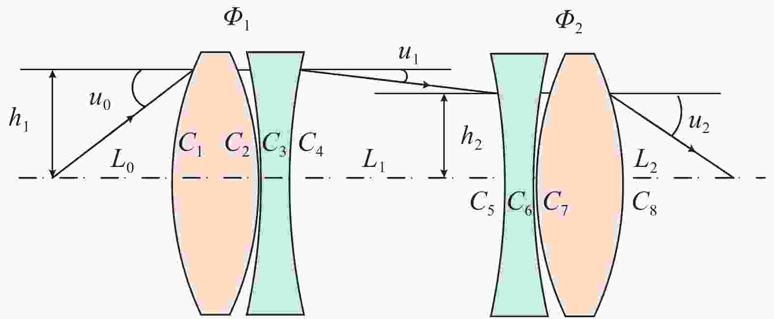
图 2 显微光学系统结构示意图
Figure 2. Schematic diagram of microscope system
图中,
${\varPhi _1}$ 和${\varPhi _2}$ 为两组元的光焦度,${L_1}$ 为两组元之间的距离,${h_1}$ 和${h_2}$ 分别为入射到第一组元和第二组元的光线高度,${C_i}$ 则表示第$i$ 个折射面的曲率。根据光焦度分配原则可计算中继系统初始结构,结果如表3所示。表 3 红外显微光学系统的初始结构参数
Table 3. Initial structural parameters of infrared microscope system
Φ1(f1′=20 mm) Φ2(f2′=20 mm) 1 2 3 4 Material Si Ge Ge Si Focal length/mm 11.186 −25.381 −25.381 11.186 Curvature radius of
the front surface/mm54.260 −153.528 −153.528 54.260 Curvature radius of
the back surface/mm−54.260 153.528 153.528 −54.260 -
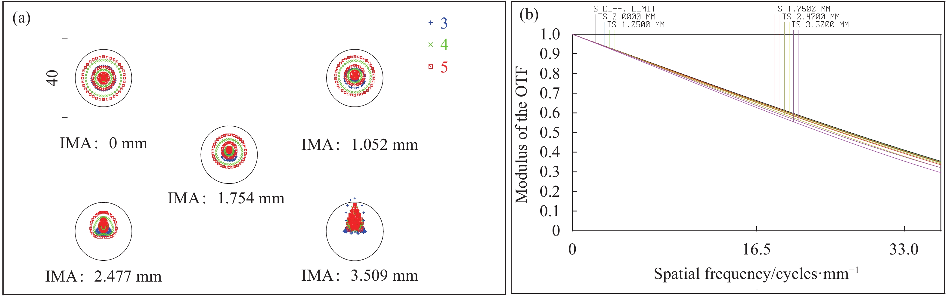
采用传统方法优化红外显微光学系统的结构图如图3所示,图4(a)、(b)分别为利用点列图和MTF曲线对像质进行评价。可以看出,各视场的弥散斑均小于单个像元尺寸,且MTF曲线接近衍射极限,其像质良好。

图 3 传统方法优化后显微光学系统结构示意图
Figure 3. Layout of the optimized system using the conventional method
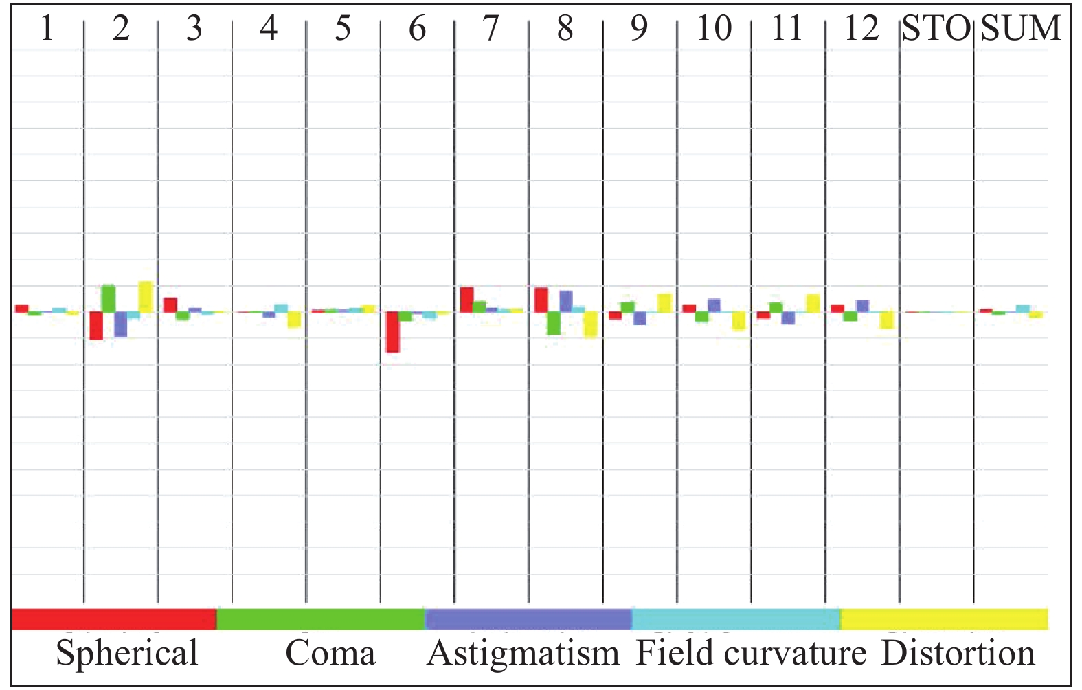
图5为显微光学系统的各个元件表面所承担的初级像差系数,其中2、3面的彗差(W131)、像散(W222)和畸变(W311)较大,表明这两个表面更加敏感,使显微光学系统更难于加工与装调。为此,应用小像差互补设计的方法来改善此状况。

图 4 传统方法优化的红外显微光学系统结构的像质((a)点列图;(b)MTF曲线)
Figure 4. Image quality obtained with the conventional optimization method ((a) Spot diagram; (b) MTF curves)

图 5 传统方法优化红外显微光学系统的初级像差系数图
Figure 5. Bar chart of primary aberration coefficients for each surface of the system obtained using conventional optimization method
-
将ZPL宏作为优化函数嵌入到优化软件中,对红外显微光学系统进行优化,得到如图6所示的光路结构。

图 6 应用小像差互补设计方法优化后的显微光学系统结构示意图
Figure 6. Layout of the optimized system using lower aberration compensation design method
利用点列图和MTF曲线对像质进行评价,如图7所示。可以看出,各视场的弥散斑均小于单个像元尺寸,且MTF曲线接近衍射极限,则像质良好。
图8为应用小像差互补设计方法优化后系统的初级像差系数分布,对比图5,可看出第2、3面的像差系数有所减小,则说明在同样满足设计要求的情况下,相对比于传统方法,用小像差互补设计方法在优化时每个面承担的像差较为均衡,在加工时会有更加宽松的元件公差,加工技术不会那么严苛,避免了个别表面承担过大像差的情况,应用该方法优化后的显微系统更容易装调并具有可重复工艺性。

图 7 小像差互补设计方法优化的红外显微光学系统结构的像质((a)点列图;(b) MTF曲线)
Figure 7. Image quality obtained with lower aberration compensation design method ((a) Spot diagram; (b) MTF curves)

图 8 小像差互补设计方法优化的显微光学系统的初级像差系数分布
Figure 8. Bar chart of primary aberration coefficients for each surface of the system obtained using lower aberration compensation design method
-
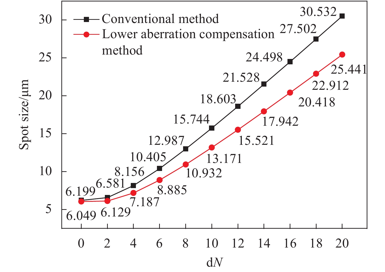
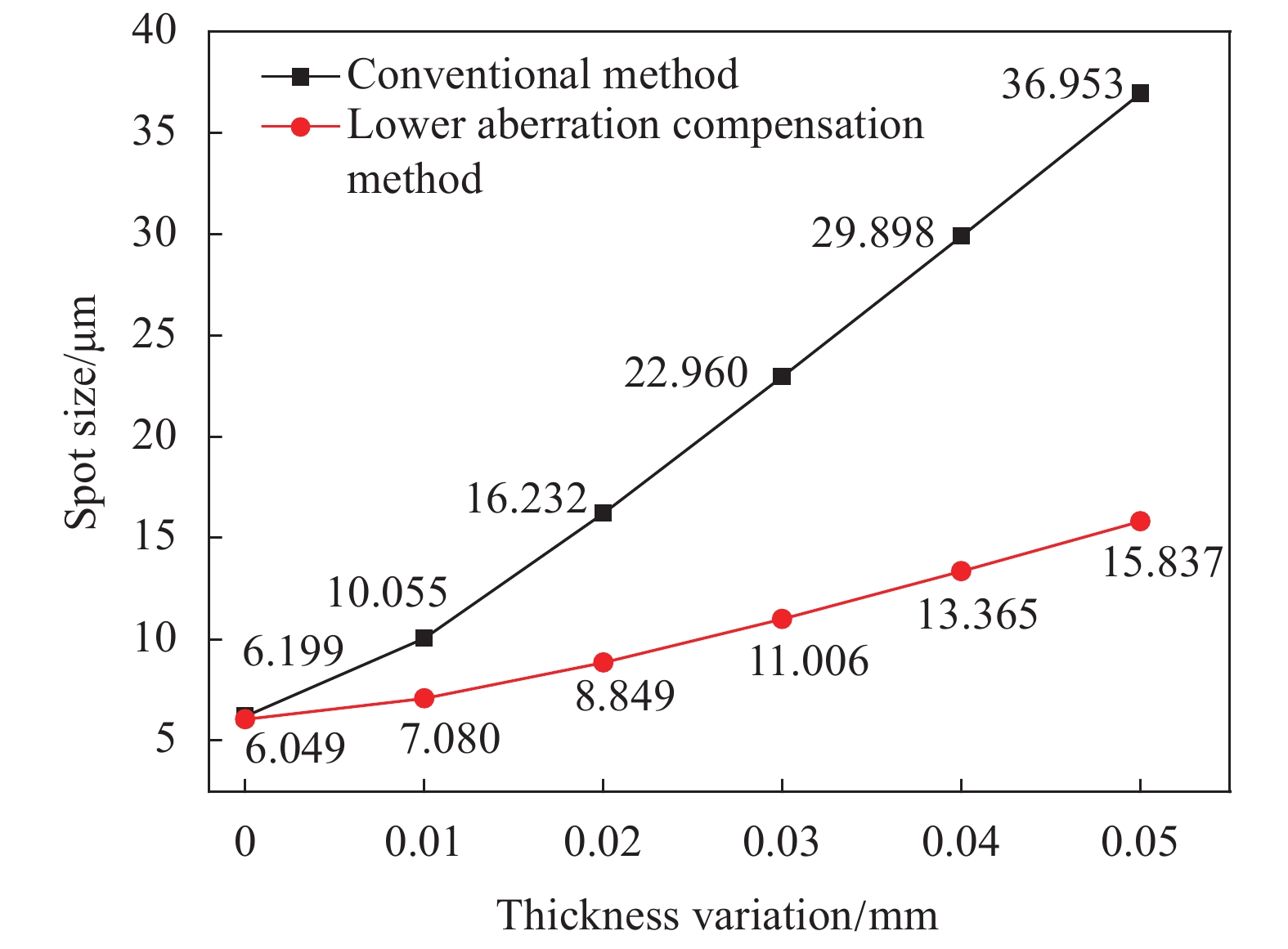
为进一步说明应用小像差互补设计方法优化光学系统的优势,用两种方法分别对其敏感的表面,即第二面进行相同的公差变化,并观察像质如弥散斑尺寸对应的变化情况。
一种方法是分别对表4~5两种优化方法的镜头数据中第二面的半径进行相同光圈数的改变,即改变第二个面的面型;第二种方法是分别对表4~5两种优化方法的镜头数据中第二面进行相同的厚度变化,即改变其与前一个面的间距,变化数值如表6所示,并观察相应的弥散斑变化,如图9~10所示。
表 4 传统方法优化的镜头数据
Table 4. Lens data obtained using the conventional optimization method
Surf: Type Radius/mm Thickness/mm Material OBJ standard Infinity 14.343 1 standard −92.197 2.000 Germanium 2 standard 51.657 2.139 3 standard −225.229 4.000 Silicon 4 standard −24.218 26.000 5 standard 44.422 2.000 Germanium 6 standard 30.170 1.500 7 standard 84.877 3.000 Silicon 8 standard −59.564 7.596 9 standard Infinity 1.000 Silicon 10 standard Infinity 2.000 11 standard Infinity 0.300 Germanium 12 standard Infinity 0.500 STO standard Infinity 20.270 IMA standard Infinity − 表 5 应用小像差互补设计方法优化的镜头数据
Table 5. Lens data obtained using lower aberration compensation design method
Surf: Type Radius/mm Thickness/mm Material OBJ standard Infinity 12.791 1 standard 50.549 4.000 Germanium 2 standard 29.345 1.072 3 standard −92.994 3.900 Silicon 4 standard −25.535 18.500 5 standard 53.868 2.800 Germanium 6 standard 30.813 1.682 7 standard 86.243 2.900 Silicon 8 standard −39.279 2.236 9 standard Infinity 1.000 Silicon 10 standard Infinity 2.000 11 standard Infinity 0.300 Germanium 12 standard Infinity 0.500 STO standard Infinity 20.270 IMA standard Infinity − 表 6 不同方法下的镜头数据变化
Table 6. Change range of lens data under different methods
Radius/mm Thickness/mm Conventional method 50.638-51.657 2.139-2.189 Lower aberration compensation method 28.961-29.345 1.072-1.122 
图 9 两种方法改变的光圈数量dN与弥散斑大小的关系图
Figure 9. Relationship between dN and the spot size in the two methods

图 10 厚度改变量与弥散斑大小的关系图
Figure 10. Relationship between thickness variation and the spot size in the two methods
从图9可以看出,在对两种方法结构的第二个面改变了相同的光圈数后,小像差互补设计法比传统方法的弥散斑的变化更小。其中,dN为光圈的改变数量。
同样的,从图10可以看出对两种方法结构的第二个面改变了相同的厚度,小像差互补设计方法与传统方法相比,其弥散斑尺寸变化幅度明显降低。
由此可知,在进行相同的改变后,无论是改变相同的面型还是相同的间距,使用小像差互补设计方法的弥散斑的改变量比传统方法的改变量小很多,即小像差互补设计方法优化后的像质稳定性更好,说明小像差互补设计方法能有效降低光学元件的公差敏感性,降低了对装调工艺的要求。
-
针对显微光学系统高分辨率与高成像质量要求,片数多且存在装调困难的特点,提出了小像差互补的设计思想,建立了相应的数学模型,并以宏语言方式将其嵌入设计软件中进行优化。以一红外显微光学系统为例,分别采用传统方法与小像差互补设计方法对其进行优化设计,并且引入相似的部件公差变化,对比分析小像差互补设计方法应用前后的优化结果和公差敏感度,发现应用小像差互补设计方法的光学系统,各元件的公差敏感度明显降低,表现出的公差范围更为宽松,加工与装调的难度与成本均得到大幅降低,验证了所提方法的有效性,则说明该方法可适用于复杂的显微光学系统,在一定程度上解决了不能同时满足高成像质量与装调要求高的矛盾,也提高了整体光学系统的稳定性和可重复性。
Design method of infrared microscope optical system with lower aberration compensation
-
摘要: 针对显微系统具有高分辨率与高成像质量的要求,其系统一般片数多装调困难,导致系统存在实际的装调效果与设计结果之间难以匹配的问题,因此提出了小像差互补的方法对系统进行设计。首先,建立基于小像差互补设计方法的数学模型,然后将其编写为可用于控制ZEMAX软件的宏语言(ZPL),再对光学系统进行优化设计。最后以一红外显微光学系统为例,对比小像差互补设计方法使用前后的优化结果,对小像差互补设计方法进行了验证,发现应用小像差互补设计方法的光学系统,总体成像质量具有突出优势,各元件的公差敏感性明显降低,整体光学系统的稳定性得到了有效提高。Abstract: Aiming at the requirements of high resolution and high imaging quality of the microscope system, the general number of pieces of the system is difficult to adjust, so that the system is difficult to match the actual adjustment result and the design result. Therefore, the lower aberration compensation design method was proposed to design the system. At the same time, the sensitivity of each optical component in a system could be reduced. First, a mathematical model of the lower aberration compensation design method was established, and then it was written into ZEMAX programming language (ZPL) macro that could be used to control ZEMAX to optimize the optical system. Finally, an infrared microscope system was taken as an example. Comparing the optimization results before and after the implementation of the lower aberration compensation design method, it was validated that the proposed method was efficient. It is found that the optical system using the lower aberration compensation design method has an outstanding advantage in image quality comparing with the conventional method. The tolerance sensitivity of each component is significantly reduced, thereby improving the stability of the overall optical system effectively.
-
图 3 传统方法优化后显微光学系统结构示意图
Figure 3. Layout of the optimized system using the conventional method
(1-object, 2, 3, 4, 5, 6, 7-lens, 8- aperture stop, 9- image surface)
图 4 传统方法优化的红外显微光学系统结构的像质((a)点列图;(b)MTF曲线)
Figure 4. Image quality obtained with the conventional optimization method ((a) Spot diagram; (b) MTF curves)
图 5 传统方法优化红外显微光学系统的初级像差系数图
Figure 5. Bar chart of primary aberration coefficients for each surface of the system obtained using conventional optimization method
图 6 应用小像差互补设计方法优化后的显微光学系统结构示意图
Figure 6. Layout of the optimized system using lower aberration compensation design method
(1-object, 2, 3, 4, 5, 6, 7-lens, 8- aperture stop, 9- image surface)
图 7 小像差互补设计方法优化的红外显微光学系统结构的像质((a)点列图;(b) MTF曲线)
Figure 7. Image quality obtained with lower aberration compensation design method ((a) Spot diagram; (b) MTF curves)
图 8 小像差互补设计方法优化的显微光学系统的初级像差系数分布
Figure 8. Bar chart of primary aberration coefficients for each surface of the system obtained using lower aberration compensation design method
图 9 两种方法改变的光圈数量dN与弥散斑大小的关系图
Figure 9. Relationship between dN and the spot size in the two methods
图 10 厚度改变量与弥散斑大小的关系图
Figure 10. Relationship between thickness variation and the spot size in the two methods
表 1 两种面型五种单色像差的波像差系数
Table 1. Coefficients in five kinds of monochromatic aberrations on two surfaces
Spherical
aberrationComa Astigmatism Field
curvatureDistortion Refractive
sphere surfaceass acs aas ads ats Refractive
conic surfaceasc acc aac adc atc  下载: 导出CSV
表 2 红外显微光学系统的设计参数
Table 2. Parameters of infrared microscope system
Parameter Value Band range/μm 3–5 NA 0.125 System F# 4.0 Detector image 640×480 Pixel size/μm 15
下载: 导出CSV
表 3 红外显微光学系统的初始结构参数
Table 3. Initial structural parameters of infrared microscope system
Φ1(f1′=20 mm) Φ2(f2′=20 mm) 1 2 3 4 Material Si Ge Ge Si Focal length/mm 11.186 −25.381 −25.381 11.186 Curvature radius of
the front surface/mm54.260 −153.528 −153.528 54.260 Curvature radius of
the back surface/mm−54.260 153.528 153.528 −54.260
下载: 导出CSV
表 4 传统方法优化的镜头数据
Table 4. Lens data obtained using the conventional optimization method
Surf: Type Radius/mm Thickness/mm Material OBJ standard Infinity 14.343 1 standard −92.197 2.000 Germanium 2 standard 51.657 2.139 3 standard −225.229 4.000 Silicon 4 standard −24.218 26.000 5 standard 44.422 2.000 Germanium 6 standard 30.170 1.500 7 standard 84.877 3.000 Silicon 8 standard −59.564 7.596 9 standard Infinity 1.000 Silicon 10 standard Infinity 2.000 11 standard Infinity 0.300 Germanium 12 standard Infinity 0.500 STO standard Infinity 20.270 IMA standard Infinity −
下载: 导出CSV
表 5 应用小像差互补设计方法优化的镜头数据
Table 5. Lens data obtained using lower aberration compensation design method
Surf: Type Radius/mm Thickness/mm Material OBJ standard Infinity 12.791 1 standard 50.549 4.000 Germanium 2 standard 29.345 1.072 3 standard −92.994 3.900 Silicon 4 standard −25.535 18.500 5 standard 53.868 2.800 Germanium 6 standard 30.813 1.682 7 standard 86.243 2.900 Silicon 8 standard −39.279 2.236 9 standard Infinity 1.000 Silicon 10 standard Infinity 2.000 11 standard Infinity 0.300 Germanium 12 standard Infinity 0.500 STO standard Infinity 20.270 IMA standard Infinity −
下载: 导出CSV
表 6 不同方法下的镜头数据变化
Table 6. Change range of lens data under different methods
Radius/mm Thickness/mm Conventional method 50.638-51.657 2.139-2.189 Lower aberration compensation method 28.961-29.345 1.072-1.122
下载: 导出CSV
-
[1] Zhang Bozhi, Gao Meijing, Rosin P L, et al. Adaptive position calibration technique for an optical micro-scanning thermal microscope imaging system [J]. Infrared Physics and Technology, 2020, 105: 103186. doi: 10.1016/j.infrared.2020.103186 [2] Zhao Huangxuan, Ke Ziwen, Chen Ningbo, et al. A new deep learning method for image deblurring in optical microscopic systems [J]. Journal of Biophotonics, 2020, 13(3): e201960147. doi: 10.1002/jbio.201960147 [3] Choi Samuel, Nin Fumiaki, Ota Takeru, et al. In vivo tomographic visualization of intracochlear vibration using a supercontinuum multifrequency-swept optical coherence microscope [J]. Biomedical Optics Express, 2019, 10(7): 3317-3342. doi: 10.1364/BOE.10.003317 [4] 薛金来, 巩岩, 李佃蒙. N. A. 0.75平场复消色差显微物镜光学设计[J]. 中国光学, 2015, 8(12): 957-963. doi: 10.3788/CO.20150806.0957 Xue Jinlai, Gong Yan, Li Dianmeng. Optical design of the N. A. 0.75 plan-apochromatic microscope objective [J]. Chinese Optics, 2015, 8(12): 957-963. (in Chinese) doi: 10.3788/CO.20150806.0957 [5] Wang Jiaoyang, Wang Lin, Yang Ying, et al. An integral design strategy combining optical system and image processing to obtain high resolution images[C]//Proceedings of SPIE, 2016, 9874: 98740F. [6] 张子辉, 王淑荣, 黄煜. 基于液体透镜自动聚焦显微成像系统设计[J]. 光电子, 2018, 8(3): 131-139. doi: 10.12677/oe.2018.83018 Zhang Zihui, Wang Shurong, Huang Yu. Auto-focus technique of microimaging system based on liquid lens [J]. Optoelectronics, 2018, 8(3): 131-139. (in Chinese) doi: 10.12677/oe.2018.83018 [7] 张佳琳, 陈钱, 张翔宇, 等. 无透镜片上显微成像技术: 理论、发展与应用[J]. 红外与激光工程, 2019, 48(6): 0603009. Zhang Jialin, Chen Qian, Zhang Xiangyu, et al. Lens-free on-chip microscopy: theory, advances, and applications [J]. Infrared and Laser Engineering, 2019, 48(6): 0603009. (in Chinese) [8] Mahajan V N. Optical Imaging and Aberrations: Part I: Ray Geometrical Optics[M]. Washington: SPIE Press, 1998: 141-242. -

 点击查看大图

计量
- 文章访问数: 449
- HTML全文浏览量: 133
- PDF下载量: 71
- 被引次数: 0