


 下载:
下载:


-
可集成的高性能纳米激光器在光通信等领域有着重要的应用前景[1-3]。层状的过渡金属硫族化合物(Transition Metal Chalcogenides, TMDs)由于具有原子层厚度、较大的激子结合能等优势[4],可以显著降低基于TMDs的微腔纳米激光器的尺寸,提高芯片的集成度[5-9]。然而,传统基于二维材料转移方法制备的基于TMDs的微腔激光器只适用于实验室研究[10-15],无法规模化制备。基于以上背景,笔者课题组提出了一种利用直接生长方法制备的Si3N4/WS2/Al2O3三明治型纳米激光器阵列[16]。基于实验结果,对该纳米激光器进行了仿真模型的构建并对关键参数进一步进行仿真优化,并展示部分器件的表征结果。该工作对光通信等领域可规模制备的高性能纳米激光器具有一定的指导意义。
-
基于直接生长方法制备的三明治型纳米激光器阵列加工流程如图1所示。在前期制备好的高品质因子(Q值)的悬空Si3N4微盘上通过物理气相沉积(Physical Vapor Deposition, PVD)的方法生长单层硫化钨(WS2),作为纳米激光器中的增益材料;为了保证单层WS2能在激光泵浦条件下稳定工作,同时为了保证单层增益材料中更大的光学限制因子,在单层WS2生长完成后,借助原子层沉积(Atomic Layer Deposition, ALD)的方法在WS2层上沉积一定厚度的氧化铝(Al2O3),制备出Si3N4/WS2/Al2O3三明治型纳米激光器阵列。

图 1 利用PVD和ALD制备Si3N4/WS2/Al2O3三明治型纳米激光器阵列流程示意图
Figure 1. Schematic diagram of preparing the Si3N4/WS2/Al2O3 sandwich nanolaser array by PVD and ALD
-
对于该Si3N4/WS2/Al2O3三明治型纳米激光器,光学限制因子$\varGamma $可以表示为:
$$ \varGamma {\text{ = }}\left( {{{\int_{{\rm{W}}{{\rm{S}}_2}} {{\varepsilon _{{\rm{W}}{{\rm{S}}_2}}}\left| {{E_\parallel }} \right|} }^2}{\rm{d}}V} \right)\bigg/\left( {{{\int_V {\varepsilon \left| E \right|} }^2}{\rm{d}}V} \right) $$ (1) 式中:$ \varepsilon $为介电常数;E为电场强度。
光学限制因子可以理解为局域在有源层中的能量(单层WS2)与器件中整体能量的比值。公式(1)中的dV表示对体积的积分,其中单层WS2的厚度为0.65 nm。
-
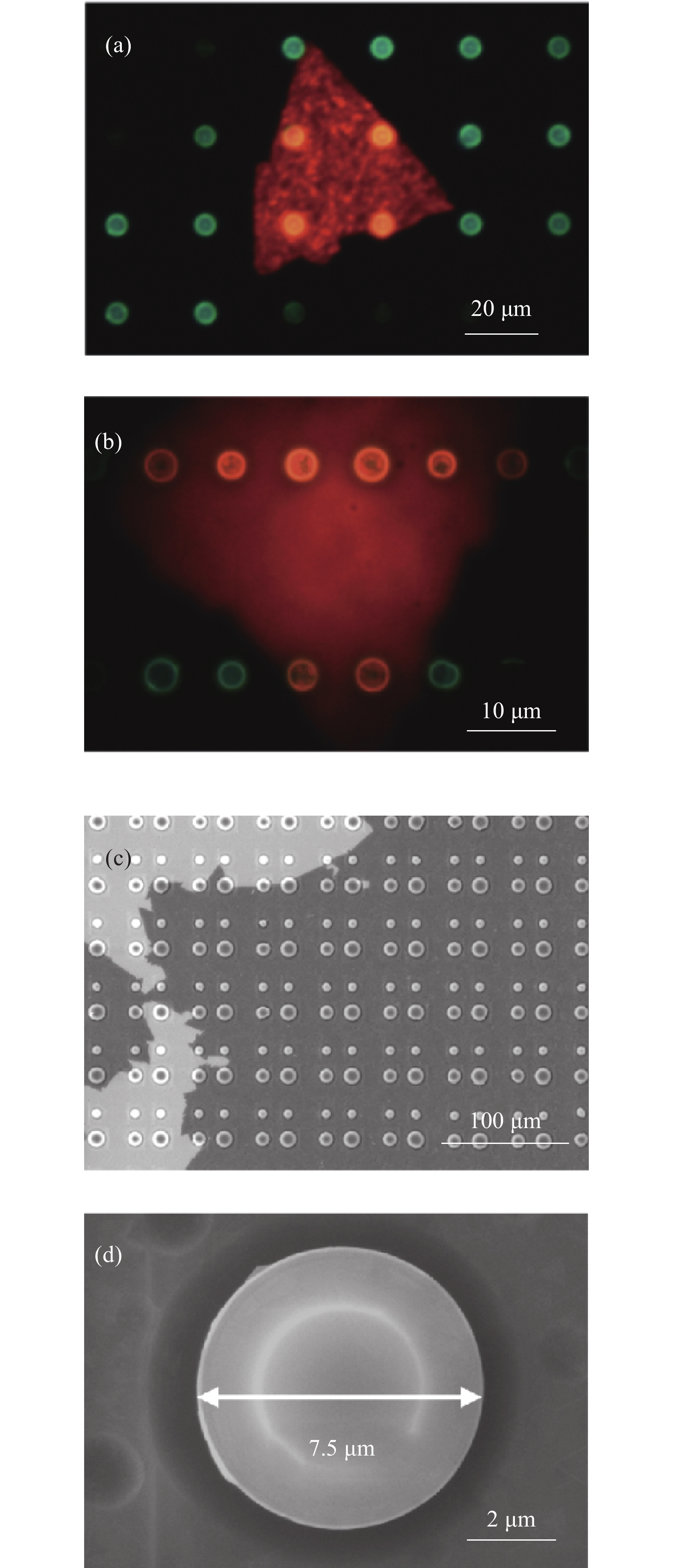
不同于传统的二维材料转移方式,利用这种直接生长的方式,可以在Si3N4微盘的上表面、边缘和下表面都生长单层的增益材料,如图2(a)所示。由于Si3N4微盘下方的氧化硅(SiO2)支柱不会对位于微盘边缘的回音壁模式(Whispering Gallery Modes,WGMs)产生影响,所以在构建仿真模型时省去了SiO2支柱结构。其次,在构建的如图2(b)所示的简化模型中,也省略了因SiO2支柱导致的WS2的圆形缺口。由于仿真模型中有源区的体积要略大于实际器件中的有源区体积,仿真计算所得的光学限制因子也会略大于实际器件中的数值。但是微盘腔的WGMs主要分布在微盘边缘,因此这种简化处理不会对最终的结论产生影响,被WS2完全包裹的微盘与底部有WS2缺口的微盘,其性能基本不会有差别。
前期的实验中,在Al2O3覆盖层厚度为130 nm、Si3N4微盘直径为300 nm、Si3N4微盘厚度为300 nm的三明治型纳米激光器中观察到了室温激射行为。基于以上实验中的初步结果,文中将进一步分析Al2O3覆盖层的厚度T、Si3N4微盘直径D以及厚度H对光学限制因子的影响,为后期器件参数的优化提供指导。

图 2 (a) Si3N4/WS2/Al2O3三明治型纳米激光器结构示意图;(b) 用于仿真分析简化模型示意图
Figure 2. (a) Structural diagram of the Si3N4/WS2/Al2O3 sandwich nanolaser; (b) Simplified model diagram for the simulation analysis
-
图3为T = 130 nm、D = 7 μm、H = 300 nm时该纳米激光器的本征横电(TE)模式,其中图3(a)为基TE径向模式,图3(b)和(c)为高阶TE径向模式。为便于分析,下文对限制因子的分析如果不做特殊说明均针对于基TE径向模式。

图 3 Si3N4/WS2/Al2O3三明治型纳米激光器结构的 (a) 基TE径向模式和(b)~(c) 高阶TE径向模式。标尺:2 μm
Figure 3. (a) Fundamental TE radial mode and (b)-(c) high-order TE radial mode of the Si3N4/WS2/Al2O3 sandwich nanolaser. Scale bar: 2 μm
-
图4为光学限制因子随着Al2O3覆盖层厚度T的变化。D = 7 μm,H = 300 nm保持不变。从图4中可以看出,当Al2O3覆盖层的厚度T为90 nm时,光学限制因子为3.63%;随着T的增加,光学限制因子也随之增加;当T为120 nm时,光学限制因子为4.34%;当T进一步增加,光学限制因子有下降的趋势,说明覆盖层厚度的增加并不能一直增加光学限制因子,同时还会增加器件的尺寸。图5所示为不同Al2O3覆盖层厚度条件下器件本征TE电场分布的侧视图。从图5中可以看出,在Al2O3覆盖层的厚度从90 nm增加到120 nm的过程中,微盘中WGMs场强最大的位置有明显的向右移动趋势。微盘中的光学模式与单层增益材料的相互作用变强,这也就从光学模式分布的角度解释了为什么随着Al2O3覆盖层厚度的增加光学限制因子也随之增加;当Al2O3覆盖层的厚度进一步增加时,可以看出微盘中的WGMs不再出现向微盘边缘移动的现象,此时光学限制因子有一定的下降趋势,但仍处于较高的数值范围内(>4.2%)。

图 4 Si3N4/WS2/Al2O3三明治型纳米激光器光学限制因子随Al2O3覆盖层厚度T的变化
Figure 4. Variation of optical confinement factor of the Si3N4/WS2/Al2O3 sandwich nanolaser with Al2O3 coating thickness T

图 5 不同Al2O3覆盖层厚度条件下Si3N4/WS2/Al2O3三明治型纳米激光器电场分布的侧视图。标尺:300 nm
Figure 5. Side view of electric field distribution of the Si3N4/WS2/Al2O3 sandwich nanolaser with different Al2O3 coating thickness. Scale bar: 300 nm
-
下面分析Si3N4微盘直径D对光学限制因子的影响。分析参数D的影响时,基于前期实验中的结果,保持T = 130 nm,H = 300 nm不变。从图6中可以看出,当微盘直径D$\leqslant $6 μm时,随着微盘直径的增加,光学限制因子也随之增加;当微盘直径D>6 μm时,限制因子有一定的下降。当微盘直径D在4.0~7.0 μm范围内变化,限制因子的数值均大于4.1%。

图 6 Si3N4/WS2/Al2O3三明治型纳米激光器光学限制因子随Si3N4微盘直径D的变化
Figure 6. Variation of optical confinement factor of the Si3N4/WS2/Al2O3 sandwich nanolaser with Si3N4 microdisk diameter D
-
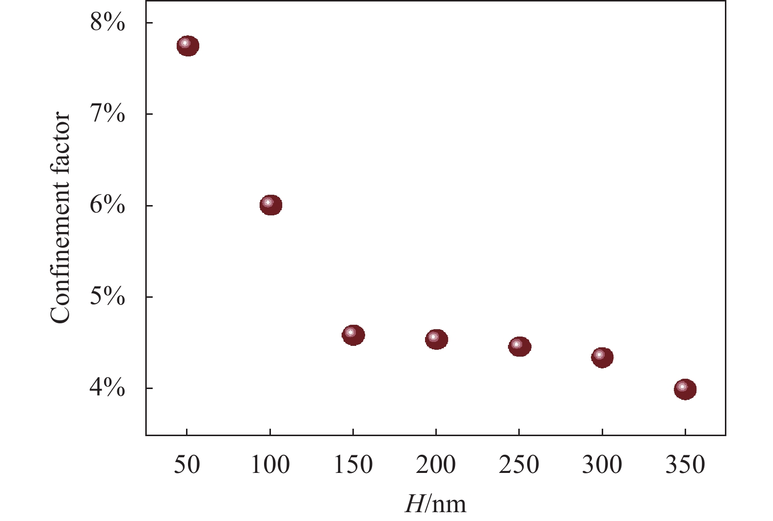
下面分析Si3N4微盘厚度H对光学限制因子的影响。分析微盘厚度H的影响时,同样基于之前实验中的参数,T = 130 nm,D = 7 μm保持不变。从图7中可以看出,当微盘厚度减小时,光学限制因子随之增加;当微盘厚度小于150 nm时,减小微盘厚度对限制因子的增加效果更为显著。尽管从理论上分析,Si3N4微盘的厚度减小时,光学限制因子有明显的提升效果,但是由于Si3N4微盘在实验中是悬空于SiO2支柱的上方,微盘厚度的减小将显著降低器件的稳定性,器件制备的难度也将显著提升。

图 7 Si3N4/WS2/Al2O3三明治型纳米激光器光学限制因子随Si3N4微盘厚度H的变化
Figure 7. Variation of optical confinement factor of the Si3N4/WS2/Al2O3 sandwich nanolaser with Si3N4 microdisk thickness H
-
借助PVD方法直接在悬空的Si3N4微盘上生长层状WS2后所得器件的表征结果如图8所示。图8(a)和图8(b)为器件的光致发光(PL)图,图8(c)为在微盘阵列上生长层状WS2后的扫描电子显微镜(SEM)图像;图8(d)为单个Si3N4/WS2微盘的SEM图。从图8中可以看出,在多个微盘上借助PVD方法直接生长单层增益材料制备纳米激光器是可行的。

图 8 借助PVD方法在Si3N4微盘上生长层状WS2后器件的表征结果。(a)~(b) 器件的PL图像;(c) 在微盘阵列和 (d) 单个微盘上生长WS2后的SEM表征结果
Figure 8. Characterization results of devices after layered WS2 was grown onto Si3N4 microdisks by the PVD method. (a)-(b) PL images of the device; SEM characterization results of WS2 grown onto (c) microdisk array and (d) a single microdisk
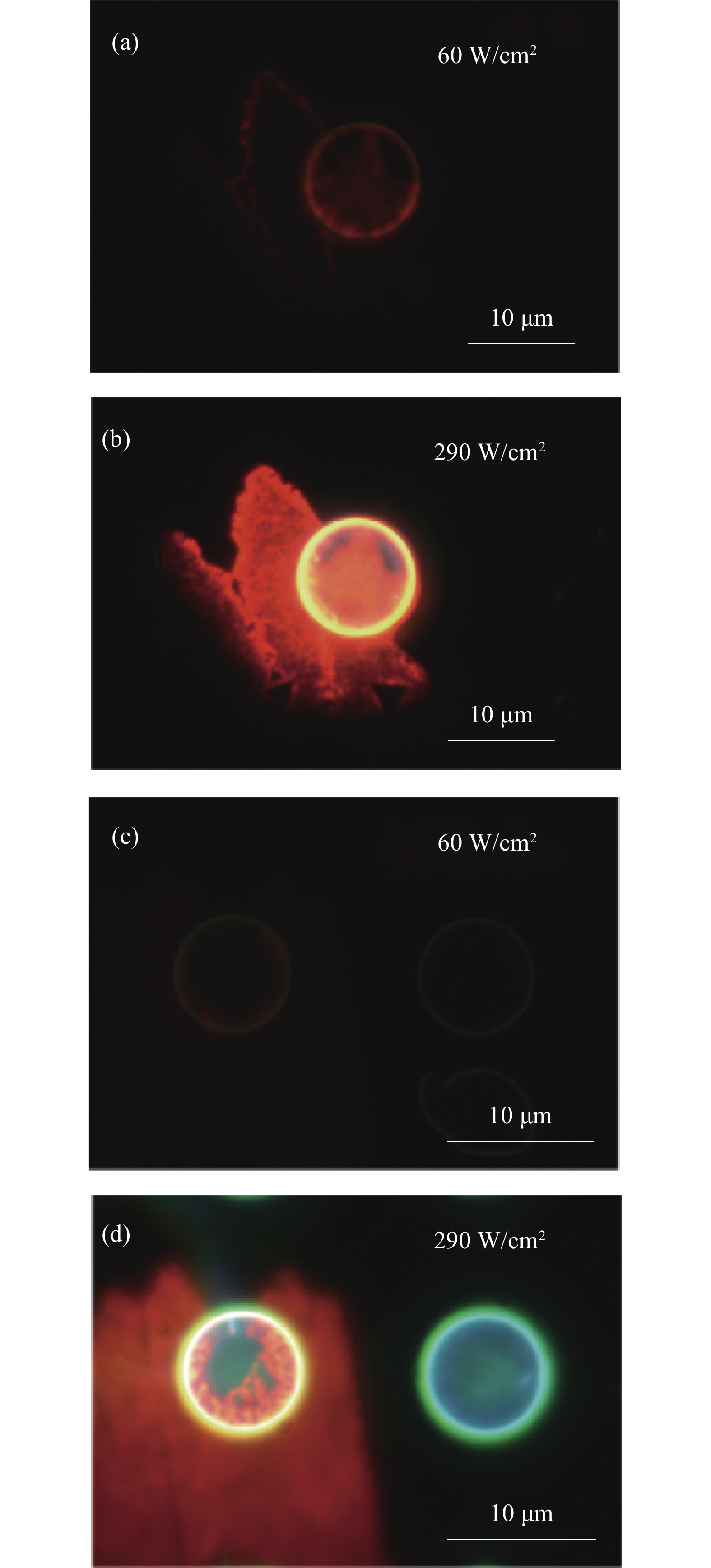
在Si3N4微盘上借助PVD方法生长WS2增益材料后,为保证器件在激光器泵浦下稳定工作以及更大的模式增益和限制因子,需要借助ALD方法在WS2上沉积Al2O3。两个覆盖有单层WS2和Al2O3覆盖层的Si3N4微盘在激光阈值以下(60 W/cm2)和以上(290 W/cm2)的实空间图像如图9所示。由于单层WS2的激子出射和位于微盘边缘WGMs之间的有效耦合,激光发射在PL图像中表现为从盘边缘出射的亮光。

图 9 Si3N4/WS2/Al2O3三明治型纳米激光器在低于阈值((a)、(c))和高于阈值((b)、(d))条件下的PL图像
Figure 9. PL images of the Si3N4/WS2/Al2O3 sandwich nanolasers below ((a), (c)) and above ((b), (d)) the lasing threshold
-
文中基于Si3N4/WS2/Al2O3三明治型纳米激光器的实验结果进行了参数仿真与优化,分析了Al2O3覆盖层T、Si3N4微盘直径D和厚度H对光学限制因子的影响。从仿真分析中可以看出,光学限制因子随着Al2O3覆盖层T以及Si3N4微盘直径D的增加先增加后减小;Si3N4微盘厚度H的减小也可以显著增加该激光器的光学限制因子。该工作为后期器件参数的进一步优化打下了良好的仿真基础,对光通信等领域可规模制备的高性能纳米激光器具有一定的指导意义。
Optimization of structural parameters of Si3N4/WS2/Al2O3 sandwich nanolaser
-
摘要: 高性能的片上纳米激光器对通信、传感以及量子等领域的发展有着至关重要的意义。纳米激光器中高的光学限制因子可以保证更大的模式增益,实现更低的激光器阈值。首先阐明了借助物理气相沉积和原子层沉积制备Si3N4/WS2/Al2O3三明治型纳米激光器阵列的工艺流程;构建了该纳米激光器的仿真模型,在仿真模型中对实际结构进行了简化并分析了Al2O3覆盖层厚度T、Si3N4微盘直径D和厚度H对光学限制因子的影响。光学限制因子随着Al2O3覆盖层T以及Si3N4微盘直径D的增加有先增加后减小的趋势,Si3N4微盘厚度H的减小也可以显著增加激光器的光学限制因子;最后展示了器件的荧光以及扫描电子显微镜的表征结果。该工作为集成光学芯片中可规模制备的高性能纳米激光器打下了良好基础。Abstract:
Objective High-performance on-chip nanolasers are very important for the development of communication, sensing, quantum and so on. On-chip nanolasers can be realized by integrating layered two-dimensional (2D) transition metal chalcogenides (TMDs) with optical microcavities. However, the integration of traditional 2D materials and microcavities is achieved by transfer methods, which limits the scale fabrication of on-chip nanolasers. Based on the above background, we propose a prototype of a TMDs-based microcavity nanolaser array prepared by direct growth method. High optical confinement factor in nanolasers can ensure a larger mode gain and a lower laser threshold. It is necessary to analyze the influence of various geometric parameters on the optical confinement factor of nanolaser by simulation and to optimize the structure, so as to lay a certain theoretical foundation for high-performance nanolasers that can be prepared on a large scale in integrated optical chips. Methods Suspended silicon nitride (Si3N4) microdisk resonators with high quality factor were prepared using complementary metal oxide semiconductor (CMOS)-compatible fabrication process; Different from traditional transfer methods to realize the integration of 2D material and microcavity, we propose to use physical vapor deposition (PVD) method to directly grow monolayer tungsten sulfide (WS2) on the surface of Si3N4 microdisk as gain material, realizing the conformal covering of the microdisk; In order to ensure that monolayer WS2 can work stably under the pump of a laser, and to ensure a larger confinement factor in the monolayer gain material, the method of atomic layer deposition (ALD) was used to deposit alumina (Al2O3) with a certain thickness, and a nanolaser with sandwich structure Si3N4/WS2/Al2O3 was formed; A simplified 3D simulation model of the nanolaser was constructed in Comsol software, and the effects of Al2O3 coating thickness T, Si3N4 microdisk diameter D and thickness H on the optical confinement factor were analyzed; The devices were characterized by fluorescence and scanning electron microscopy. Results and Discussions When constructing the simulation model, the silicon oxide (SiO2) pillar structure and the circular notch of monolayer WS2 caused by the SiO2 pillar are omitted (Fig.2); The effects of Al2O3 coating thickness T (Fig.4), Si3N4 microdisk diameter D (Fig.6) and thickness H (Fig.7) on the optical confinement factor were analyzed. Within the range of selected parameters, the optical confinement factor first increases and then decreases with the increase of Al2O3 coating thickness T and Si3N4 microdisk diameter D, the decrease of the thickness H of the Si3N4 microdisk can also significantly increase the optical confinement factor of the nanolaser; The feasibility of this direct growth method was demonstrated by fluorescence and scanning electron microscopy after monolayer WS2 was grown onto the Si3N4 microdisk (Fig.8); After the deposition of completion of Al2O3, time-space images of the nanolaser above and below the threshold were shown (Fig.9). Conclusions Nanolaser with a sandwich structure Si3N4/WS2/Al2O3 was proposed. The preparation process of the sandwich nanolaser was expounded. Suspended Si3N4 microdisk resonators with high quality factor were prepared using CMOS-compatible fabrication process, PVD method was used to directly grow monolayer WS2 on the surface of Si3N4 microdisk as gain material, and ALD method was adopted to deposit Al2O3 with a certain thickness after monolayer WS2 was grown. Thus, the nanolaser with a sandwich structure Si3N4/WS2/Al2O3 was formed; In the simulation software, the geometry of the nanolaser was simplified and the parameters were simulated and optimized, the effects of Al2O3 coating thickness T, Si3N4 microdisk diameter D and thickness H on the optical confinement factor were analyzed. Within the range of selected parameters, the optical confinement factor first increases and then decreases with the increase of Al2O3 coating thickness T and Si3N4 microdisk diameter D, the decrease of the thickness H of the Si3N4 microdisk can also significantly increase the optical confinement factor of the nanolaser; The characterization results of some devices were displayed, which lays a good simulation foundation for the further optimization of device parameters in the later period, and has certain guiding significance for the large-scale preparation of high-performance nanolasers in the field of optical communication and so on. -
图 1 利用PVD和ALD制备Si3N4/WS2/Al2O3三明治型纳米激光器阵列流程示意图
Figure 1. Schematic diagram of preparing the Si3N4/WS2/Al2O3 sandwich nanolaser array by PVD and ALD
图 2 (a) Si3N4/WS2/Al2O3三明治型纳米激光器结构示意图;(b) 用于仿真分析简化模型示意图
Figure 2. (a) Structural diagram of the Si3N4/WS2/Al2O3 sandwich nanolaser; (b) Simplified model diagram for the simulation analysis
图 3 Si3N4/WS2/Al2O3三明治型纳米激光器结构的 (a) 基TE径向模式和(b)~(c) 高阶TE径向模式。标尺:2 μm
Figure 3. (a) Fundamental TE radial mode and (b)-(c) high-order TE radial mode of the Si3N4/WS2/Al2O3 sandwich nanolaser. Scale bar: 2 μm
图 4 Si3N4/WS2/Al2O3三明治型纳米激光器光学限制因子随Al2O3覆盖层厚度T的变化
Figure 4. Variation of optical confinement factor of the Si3N4/WS2/Al2O3 sandwich nanolaser with Al2O3 coating thickness T
图 5 不同Al2O3覆盖层厚度条件下Si3N4/WS2/Al2O3三明治型纳米激光器电场分布的侧视图。标尺:300 nm
Figure 5. Side view of electric field distribution of the Si3N4/WS2/Al2O3 sandwich nanolaser with different Al2O3 coating thickness. Scale bar: 300 nm
图 6 Si3N4/WS2/Al2O3三明治型纳米激光器光学限制因子随Si3N4微盘直径D的变化
Figure 6. Variation of optical confinement factor of the Si3N4/WS2/Al2O3 sandwich nanolaser with Si3N4 microdisk diameter D
图 7 Si3N4/WS2/Al2O3三明治型纳米激光器光学限制因子随Si3N4微盘厚度H的变化
Figure 7. Variation of optical confinement factor of the Si3N4/WS2/Al2O3 sandwich nanolaser with Si3N4 microdisk thickness H
图 8 借助PVD方法在Si3N4微盘上生长层状WS2后器件的表征结果。(a)~(b) 器件的PL图像;(c) 在微盘阵列和 (d) 单个微盘上生长WS2后的SEM表征结果
Figure 8. Characterization results of devices after layered WS2 was grown onto Si3N4 microdisks by the PVD method. (a)-(b) PL images of the device; SEM characterization results of WS2 grown onto (c) microdisk array and (d) a single microdisk
-
[1] Ning Cunzheng. Semiconductor nanolasers and the size-energy-efficiency challenge: a review [J]. Advanced Photonics, 2019, 1(1): 014002. doi: 10.1117/1.AP.1.1.014002 [2] Atabaki A H, Moazeni S, Pavanello F, et al. Integrating photonics with silicon nanoelectronics for the next generation of systems on a chip [J]. Nature, 2018, 556(7701): 349-354. doi: 10.1038/s41586-018-0028-z [3] Cheng Q, Bahadori M, Glick M, et al. Recent advances in optical technologies for data centers: a review [J]. Optica, 2018, 5(11): 1354-1370. doi: 10.1364/OPTICA.5.001354 [4] Xia F, Wang H, Xiao D, et al. Two-dimensional material nanophotonics [J]. Nature Photonics, 2014, 8(12): 899-907. doi: 10.1038/nphoton.2014.271 [5] Wang L, Zhou X, Yang S, et al. 2D-material-integrated whispering-gallery-mode microcavity [J]. Photonics Research, 2019, 7(8): 905-916. doi: 10.1364/PRJ.7.000905 [6] Du W, Li C, Sun, J, et al. Nanolasers based on 2D materials [J]. Laser & Photonics Reviews, 2020, 14(12): 2000271. doi: 10.1002/lpor.202000271 [7] Li Y, Sun H, Gan L, et al. Optical properties and light-emission device applications of 2D layered semiconductors [J]. Proceedings of the IEEE, 2020, 108(5): 676-703. doi: 10.1109/JPROC.2019.2936424 [8] You J, Luo Y, Yang J, et al. Hybrid/Integrated silicon photonics based on 2D materials in optical communication nanosystems [J]. Laser & Photonics Reviews, 2020, 14(12): 2000239. doi: 10.1002/lpor.202000239 [9] Liu D S, Wu J, Xu H, et al. Emerging light-emitting materials for photonic integration [J]. Advanced Materials, 2021, 33(4): 2003733. doi: 10.1002/adma.202003733 [10] Reed J C, Zhu A Y, Zhu H, et al. Wavelength tunable microdisk cavity light source with a chemically enhanced MoS2 emitter [J]. Nano Letters, 2015, 15(3): 1967-1971. doi: 10.1021/nl5048303 [11] Wu S, Buckley S, Schaibley J R, et al. Monolayer semiconductor nanocavity lasers with ultralow thresholds [J]. Nature, 2015, 520(7545): 69-72. doi: 10.1038/nature14290 [12] Ye Y, Wong Z J, Lu X, et al. Monolayer excitonic laser [J]. Nature Photonics, 2015, 9(11): 733-737. doi: 10.1038/nphoton.2015.197 [13] Li Y, Zhang J, Huang D, et al. Room-temperature continuous-wave lasing from monolayer molybdenum ditelluride integrated with a silicon nanobeam cavity [J]. Nature Nanotechnology, 2017, 12(10): 987-992. doi: 10.1038/nnano.2017.128 [14] Fang H, Liu J, Li H, et al. 1 305 nm few-layer MoTe2-on-silicon laser-like emission [J]. Laser & Photonics Reviews, 2018, 12(6): 1800015. doi: 10.1002/lpor.201800015 [15] Liu Y, Fang H, Rasmita A, et al. Room temperature nanocavity laser with interlayer excitons in 2D heterostructures [J]. Science Advances, 2019, 5(4): eaav4506. doi: 10.1126/sciadv.aav4506 [16] Liu N, Yang X, Zhang J, et al. Room-temperature excitonic nanolaser array with directly grown monolayer WS2 [J]. ACS Photonics, 2023, 10(1): 283-289. doi: 10.1021/acsphotonics.2c01618 -

 点击查看大图

计量
- 文章访问数: 211
- HTML全文浏览量: 58
- PDF下载量: 31
- 被引次数: 0

