


-
红外探测器在空间科学、军事装备、工业生产等应用领域占据着重要地位,技术需求推动着探测器向高性能、低成本的方向发展。传统的红外探测器材料体系有InSb[1]、量子阱[2]、碲镉汞[3]。其中,碲镉汞红外探测器性能较好,但对于碲镉汞长波探测器,需要更高组分的汞,材料外延难度更大,对材料生长质量以及器件工艺要求更加严格,导致成品率低下[4],目前业内实际状况是碲镉汞长波探测器焦平面的良率为10%左右,其器件成本较高。近年来,快速发展的InAs/GaSb 超晶格红外探测器显示出巨大的优势[5],通过调整其周期结构,可以使截止波长覆盖2.7~30 µm的红外波段,有利于满足多色探测[6]的需求,如中/短波[7]、中/中波[8]、中/长波[9]、长/长波[10]等。同时,InAs/GaSb超晶格还具有量子效率高、暗电流小、材料均匀性好、工作温度高、成本低等优势,逐步成为第三代红外焦平面探测器的优选材料[11]。
相比于单色探测器件,覆盖不同大气窗口的双波段红外探测可以同时在两个波段获取目标信息[12],通过后端图像处理算法可以显著降低背景噪声对图像质量的影响,提高环境适应性,在预警系统中能明显地降低虚警率,显著地提高系统的性能[13]。因此,它被广泛地应用于军用和民用领域,比如红外夜视系统、目标识别、导弹跟踪等[14]。目前,对于二类超晶格双波段探测器最急需解决的问题是减小串扰和降低暗电流。2015年,美国西北大学报道了InAs/InAsSb二类超晶格作为吸收区的nBn结构中/长波双波段探测器,中、长波的峰值探测率为8.2×1012 、1.6×1011 cm·Hz1/2·W−1[15]。2018年,中国科学院半导体研究所牛智川等报道了NMπP-PπMN结构的中/长波双波段探测器,其中M层采用InAs/GaSb超晶格中插入AlSb层,AlSb相比于InAs和GaSb具有更宽的带隙,可以同时充当导带电子和价带空穴的势垒,从而达到减小暗电流和提高特征值RA(器件电阻与面积的乘积)的效果[16]。但其报道的器件需要较大的工作电压,因此中波的势垒区设计与掺杂框架仍有待优化。2019年,中国空空导弹研究院报道了基于PNP结构的InAs/GaSb二类超晶格中/短波双色红外焦平面探测器,通过在中波通道和长波通道之间加入GaSb层作为势垒以改善漏电性能,同时通过研究钝化工艺优化器件侧壁漏电流[17]。制备出的器件在77 K温度下,双色峰值探测率达到中波3.7×1011 cm·Hz1/2·W−1,短波2.2×1011 cm·Hz1/2·W−1。总体上,国内外对超晶格双波段探测器的研究报道比较少,尤其是在优化器件结构设计方面可参考的文献也较少。由于双波段超晶格探测器结构比较复杂,因此仿真优化对于指导器件性能的提升非常关键。
由于nBn结构的红外探测器的势垒层能够明显地降低器件的暗电流,且结构设计较为简单,能够在得到较高的探测性能的同时降低整个双波段探测结构与外延工艺的复杂性。基于此,文中通过使用SILVACO软件,较为系统地对基于nBn结构的InAs/GaSb二类超晶格中/长波双波段红外探测器进行建模仿真分析,通过比较不同结构的器件在不同偏压下的中波/长波通道的响应和暗电流大小,分析势垒层厚度、吸收层厚度、不同区域的掺杂对暗电流和串扰的影响,从而得到最佳的模型参数,设计目标是中波通道截止波长为4.8 µm,暗电流密度减小到10−4 A·cm−2,峰值探测率达到1011 cm·Hz1/2·W−1;长波通道截止波长为10 µm,暗电流密度减小到10−4 A·cm−2,峰值探测率达到1011 cm·Hz1/2·W−1;中波通道和长波通道之间的串扰减小到10%左右。相关研究结论为器件设计和加工提供理论参考,降低实验迭代的成本。
-
InAs/GaSb超晶格探测器的暗电流受温度的影响较大,高温下扩散电流为主要的暗电流机制,低温下以产生复合(Generation-recombination, GR)电流为主导机制。其中,漂移扩散电流模型是基于玻尔兹曼传输理论的推导与近似,使用漂移-扩散模型来近似连续性方程中的电流密度为:
$$ {J_{n,p}} = q(n,p){\mu _{n,p}}E \pm q{D_{n,p}}{\nabla _{n,p}} $$ (1) 式中:q为电子电荷;µ为迁移率;E为电场;D为扩散常数;n为电子浓度;p为空穴浓度。
SRH (Shockley-Read-Hall)复合电流是由缺陷引起的产生复合中心能级,产生复合中心会向导带和价带发射电子与空穴,同时导带上的电子和价带上的空穴会在产生复合中心复合,这引起的电流为SRH暗电流,对应表达式如下[18]:
$$ \begin{gathered} {R_{SRH}} = \\ \dfrac{{pn - n_{_{ie}}^2}}{{{\tau _p}\left[n + {n_{ie}}\exp \left(\dfrac{{{E_{trap}}}}{{k{T_L}}}\right)\right] + {\tau _n}\left[p + {n_{ie}}\exp \left(\dfrac{{ - {E_{trap}}}}{{k{T_L}}}\right)\right]}} \\ \end{gathered} $$ (2) $$ {J_{GR}} = q\int\limits_W {{R_{SRH}}{\rm{d}}y} $$ (3) 式中:Etrap为陷阱能级与本征费米能级的能量差;TL为晶格温度;τn和τp分别为电子、空穴的寿命;nie为本征载流子浓度;n、p为载流子浓度;k为玻耳兹曼常数;W为耗尽区宽度。
陷阱辅助隧穿电流[19] (Trap-Assisted Tunneling, TAT)是电子在陷阱的辅助下发射至导带,在上述等式中引入一个场效应因子Γ来反应声子辅助隧穿等对载流子寿命的影响,对应表达式如下[20-21]:
$$ \begin{gathered} {R_{TAT}} = \\ \dfrac{{pn - n_{_{ie}}^2}}{{\dfrac{{{\tau _p}}}{{1 + {\varGamma _p}}}\left[n + {n_{ie}}\exp \left(\dfrac{{{E_{trap}}}}{{k{T_L}}}\right)\right] + \dfrac{{{\tau _n}}}{{1 + {\varGamma _n}}}\left[p + {n_{ie}}\exp \left(\dfrac{{ - {E_{trap}}}}{{k{T_L}}}\right)\right]}} \\ \end{gathered} $$ (4) $$ {\varGamma _{n,p}} = \frac{{\Delta {E_n}}}{{k{T_L}}}\int_0^1 {\exp \left(\frac{{\Delta {E_{n,p}}}}{{k{T_L}}}u - {K_{n,p}}{u^{3/2}}\right){\rm{d}}u} $$ (5) 式中:u为积分变量;ΔEn,p为电子或空穴能够发生隧穿的能量区间。
$$ {K_{n,p}} = \frac{4}{3}\frac{{\sqrt {2{m_0}\Delta E_{n,p}^3} }}{{q\hbar \left| E \right|}} $$ (6) 式中:ћ为普朗克常数;m0为有效隧穿质量。
SILVACO器件仿真的运算模型是基于泊松方程,载流子连续性方程,输运方程。通过调用不同的模型来描述扩散电流、GR电流、隧穿电流、光生电流,其中探测器总体的暗电流会随着温度的升高而逐渐变大,但不同温度下的暗电流主导机制不同。仿真过程中将超晶格材料等效为一层体材料进行能带参数的定义,如表1和表2所示,这些参数一方面来源于文献调研[22-24],另一方面使用加权平均或由能带结构计算而来,因此这些参数大多是估算结果。按照如图1所示的仿真框架进行文中的优化仿真,后续将会通过材料和探测器的各项测试结果进而反馈分析,从而进一步优化仿真结果。
表 1 15 MLs InAs/8 MLs GaSb 超晶格材料参数等效定义
Table 1. Material parameters of 15 InAs/8 GaSb superlattice
Parameter Value Electron effective mass (x m0) 0.024 Hole effective mass (x m0) 0.104 Permittivity/F.m−1 14.985 Electron affinity/eV 4.8179 Bandgap at 300 K/eV 0.12 Electron mobility at 300 K/cm2·V−1·s−1 1000 Hole mobility at 300 K/cm2·V−1·s−1 270 表 2 8 MLs InAs/6 MLs GaSb 超晶格材料参数等效定义
Table 2. Material parameters of 8 InAs/6 GaSb superlattice
Parameter Value Electron effective mass (x m0) 0.04 Hole effective mass (x m0) 0.75 Permittivity/F.m−1 15.3 Electron affinity/eV 4.667 Bandgap at 300 K/eV 0.258 Electron mobility at 300 K/cm2·V−1·s−1 1000 Hole mobility at 300 K/cm2·V−1·s−1 500 
图 1 仿真流程框架图
Figure 1. Simulation flow frame diagram
-
根据设计目标要求,首先使用k.p方法对InAs/GaSb能带结构进行了计算,得到如图2(a)和图2(b)所示,77 K下,15 MLs InAs/8 MLs GaSb超晶格的带隙为0.123 eV,对应的截止波长为10.058 µm;8 MLs InAs/6 MLs GaSb超晶格的带隙为0.258 eV,对应的截止波长为4.815 µm。因此选用这两种超晶格分别作为双波段探测结构中的长波吸收区和中波吸收区。文中设计的中/长波双波段niBin探测器结构如图2(c)所示:从下至上依次是下接触层-长波吸收层-公共势垒层-中波吸收层-上接触层。外延工艺顺序简要介绍如下:首先,在GaSb衬底层上生长一层GaSb缓冲层用来改善界面粗糙度,实现原子台阶;接着在缓冲层上生长100 nm厚的15 MLs InAs/8 MLs GaSb超晶格,并进行1×1018 cm−3的Si掺杂,以此作为长波通道的下接触层,在下接触层上生长15 MLs InAs/8 MLs GaSb超晶格长波通道吸收层;然后,在长波吸收层上生长AlGaSb势垒层,这是长波通道和中波通道公共的势垒层,阻挡多数载流子(电子)的流通而允许少数载流子(空穴)的流通,势垒层的加入可以极大程度地减少SRH复合暗电流且抑制串扰;接着,在公共势垒层上方生长8 MLs InAs/6 MLs GaSb超晶格中波通道吸收层,在中波吸收层上方再生长100 nm的8 MLs InAs/6 MLs GaSb超晶格并进行1×1018 cm−3的Si掺杂,以此作为中波通道的上接触层;最后,分别在GaSb缓冲层上和中波通道的上接触层8 MLs InAs/6 MLs GaSb超晶格上蒸镀150 nm的Ti/Pt/Au层用来作为下电极和上电极层。器件尺寸定义为20 μm×20 μm。

图 2 (a) 15 MLs InAs/8 MLs GaSb长波超晶格的能带图;(b) 8 MLs InAs/6 MLs GaSb中波超晶格的能带图;(c)中/长波双波段红外探测器结构
Figure 2. (a) Simulated band diagram of the 15 MLs InAs/8 MLs GaSb long-wave superlattices; (b) Simulated band diagram of the 8 MLs InAs/6 MLs GaSb mid-wave superlattices; (c) Mid/long wave dual-band infrared detector structure
文中通过分析不同结构和偏压下的J-V曲线,分析势垒层、掺杂、吸收层厚度、温度对暗电流、光响应的影响,来从理论设计方面尽量减小器件的暗电流和提升量子效率。
-
探测器暗电流主要包括扩散电流、产生复合电流、直接隧穿电流、陷阱辅助隧穿电流和表面漏电流。不同的暗电流机制有不同的影响因素,暗电流的四个主要组成机制都与探测器的工作环境温度有关,温度对暗电流信号的影响起主要作用,探测器的暗电流会随着温度的降低而降低,所以抑制暗电流有效的措施是保持器件在稳定的低温环境中。通过能带设计与器件结构设计、钝化工艺等降低暗电流以提高工作温度是器件优化的重要方向。其中扩散电流与带隙的大小有关,高温下的暗电流主要以扩散电流为主。GR电流主要是SRH复合电流,可通过降低缺陷复合中心和提高吸收区的掺杂来抑制。但当掺杂浓度过大时,电场也会变大,这会在一定程度上增加隧穿电流。同时材料质量和工艺也会影响暗电流。通常低温下的表面漏电流较为显著,需要通过钝化工艺来减少此暗电流。
-
使用SILVACO软件对上述器件结构进行建模,并设置电子有效质量、电子亲和势、电子迁移率等参数。其中,将15 MLs InAs/8 MLs GaSb超晶格吸收层厚度定为4 µm,掺杂为1×1015 cm−3,8 MLs InAs/6 MLs GaSb吸收层厚度为2 µm,掺杂为1×1015 cm−3。AlxGa1−xSb的插入是为了在导带处形成了电子势垒,阻挡多子电子流通,同时价带几乎平齐,能够允许少子空穴的流动,这样的能带结构可以提高光生载流子的收集效率,降低暗电流。通过调节AlxGa1−xSb的组分,x为Al的组分,分别取0.15、0.19、0.2、0.21、0.25、0.3,得到如图3(a)所示的77 K下的能带图,图中显示x小于0.2时,AlGaSb的价带能量较高,与8 MLs InAs/6 MLs GaSb和15 MLs InAs/8 MLs GaSb超晶格吸收区形成较为明显的价带带阶;x大于0.2时,AlGaSb的价带能量较低,同样会与8 MLs InAs/6 MLs GaSb和15 MLs InAs/8 MLs GaSb形成较为明显的价带带阶;因此,取x为0.2,即势垒层为Al0.2Ga0.8Sb,得到如图3(b)所示的器件整体的能带图。

图 3 (a) 不同Al组分的AlxGa1−xSb的能带图;(b)器件整体的能带图
Figure 3. (a) Simulated band diagram of the AlxGa1−xSb with different Al components; (b) Simulated band diagram of the device
-
将15 MLs InAs/8 MLs GaSb超晶格吸收层厚度设为4 µm,掺杂为1×1015 cm−3,8 MLs InAs/6 MLs GaSb超晶格吸收层厚度为2 µm,掺杂为1×1015 cm−3,势垒层为Al0.2Ga0.8Sb。在此基础上分析势垒层厚度对暗电流的影响。厚度取10~1000 nm,由图4(a)和图4(b)所示,正偏下,随着势垒层厚度增加,中波通道暗电流逐渐减小,光电流逐渐增加,但增大的并不明显。反偏下,长波通道暗电流同样会随着势垒层厚度的增大而减小,光电流也随着势垒层厚度的增加而逐渐增加,但同时串扰也略有增大。77 K下的暗电流主导机制是SRH电流和隧穿暗电流。同样电压下,势垒层厚度增加会降低电场强度,进而减小SRH暗电流,势垒层厚度增大也会直接降低隧穿概率,进而降低隧穿暗电流,所以总的暗电流会减小。光电流随着势垒层厚度的增加而增加,这是因为降低了吸收区的电场强度进而在一定程度上减小了光生载流子的SRH复合。由于当AlGaSb的厚度过大时,会与超晶格产生较大的晶格失配应力。因此,考虑势垒层厚度对器件整体的暗电流和光响应的影响,同时简化器件结构以便于后续实际材料生长和器件工艺,一般将AlGaSb势垒层厚度定为100 nm。

图 4 (a) 77 K下不同势垒层厚度下的J-V曲线;(b) ±0.3 V下不同势垒层厚度下的光响应谱
Figure 4. (a) J-V curve under different thickness of barrier at 77 K;(b) Photoresponse simulations with different thickness of barrier at ±0.3 V
-
将15 MLs InAs/8 MLs GaSb吸收层厚度设置为4 µm,8 MLs InAs/6 MLs GaSb吸收层厚度为2 µm,势垒层Al0.2Ga0.8Sb厚度为100 nm。在此基础上研究77 K下吸收层掺杂和势垒层掺杂对器件暗电流和光响应的影响。对吸收层分别进行1×10¹⁵、1×10¹⁶、1×1017 cm−3的掺杂,图5(a)中,在0.3 V和−0.3 V的工作电压下,吸收层掺杂浓度增大时,即电子浓度增大,相应的少子空穴浓度减小,暗电流减小,但增大掺杂浓度对降低暗电流的影响较微弱,且由图5(b)可以看出高浓度掺杂减小少数载流子空穴的寿命,即带间复合率增大,使得光生载流子更多的被复合而没有被电极收集,从而降低光响应。且高浓度掺杂会使得导带上的电子浓度增大,进而增加自由载流子的光吸收,增加光损耗,从而也会降低光响应。因此,通常吸收层为非故意掺杂。通过对势垒层分别进行1×10¹⁵、1×10¹⁶、5×1016 cm−3的掺杂,由图5(c)和图5(d)可得,在0.3 V和−0.3 V的工作电压下,当势垒层掺杂增大时,暗电流会相应地微弱的减小,且基本不影响光响应。但由图5(e)可以看到,当掺杂过高时会引起较大的带阶,这会阻挡光生电子的传输,减小光电流。因此,在实际的材料生长中,采取势垒层为非故意掺杂。

图 5 (a) 吸收层在不同掺杂浓度下的暗电流密度;(b) 吸收层在不同掺杂浓度下的光响应;(c) 势垒层在不同掺杂浓度下的暗电流密度;(d) 势垒层在不同掺杂浓度下的光响应;(e) 势垒层在不同掺杂浓度下的能带图
Figure 5. (a) Dark current density simulations of absorber with different doping; (b) Photoresponse simulations of absorber with different doping; (c) Dark current simulations of absorber with different doping; (d) Photoresponse simulations of absorber with different doping; (e) Simulated band diagram of absorber with different doping concentrations
-
对于双波段器件,串扰是一个很大的问题,文中通过优化中波吸收层和长波吸收层的厚度来减小两个通道间的串扰。将15 MLs InAs/8 MLs GaSb吸收层掺杂设为1×1015 cm−3,8 MLs InAs/6 MLs GaSb吸收层掺杂设为1×1015 cm−3,势垒层Al0.2Ga0.8Sb厚度为100 nm,掺杂为1×1015 cm−3。
为量化器件中波通道与长波通道之间的光学串扰,定义参数CT如下[25]:
$$ C{T_{BA}} = \frac{{S_B'}}{{S_A}} \times 100 \text{%} $$ (7) $$ C{T_{AB}} = \frac{{S_A'}}{{S_B}} \times 100\text{%} $$ (8) 式中:CTBA为3~5 µm波段范围内长波通道对中波通道的光学串扰;CTAB为8~12 µm波段范围内中波通道对长波通道的光学串扰;SA为3~5 µm波段范围内中波通道的相对光谱响应曲线与波长轴所围成的面积;SB为8~12 µm波段范围内长波通道的相对光谱响应曲线与波长轴所围成的面积;$S_B' $为8~12 µm波段范围内长波通道的相对光谱响应曲线与波长轴所围成的面积;$S_A' $为3~5 µm波段范围内中波通道的相对光谱响应曲线与波长轴所围成的面积。通过将长波吸收区15 MLs InAs/8 MLs GaSb超晶格厚度设为2 µm,改变中波吸收区8 MLs InAs/6 MLs GaSb超晶格的厚度,得到了如图6(a)所示的光响应图:随着8 InAs/6GaSb超晶格厚度增加,中波的光电流逐渐变大,且长波通道对于中波的光响应逐渐减小,且由图6(c)可以看到,中波通道与长波通道间的串扰逐渐减小。实际在MBE生长材料的过程当中,要生长这么厚的超晶格材料,对于材料质量的把控较为困难,且后续在器件工艺时也存在较大的难度。因此将中波吸收层8 MLs InAs/6 MLs GaSb厚度设为4 µm,在一定程度上减小了串扰,但对于后续的MBE生长也带来了一定程度地挑战。

图 6 (a) 不同中波吸收层厚度下的光响应率;(b) 不同长波吸收层厚度下的光响应率;(c) 不同中波吸收层厚度下的串扰;(d) 不同长波吸收层厚度下的串扰
Figure 6. (a) Photoresponse simulations with different thickness of mid-wave absorber; (b) Photoresponse simulations with different thickness of long-wave absorber; (c) Cross talk simulations with different thickness of mid-wave absorber; (d) Cross talk simulations with different thickness of long-wave absorber
图6(b)是将中波吸收层8 MLs InAs/6 MLs GaSb超晶格厚度设为4 µm,改变长波吸收层15 MLs InAs/8 MLs GaSb超晶格的厚度,可以看到随着长波吸收层厚度的增加,长波通道的响应率也逐渐增加,中波通道的响应率没有发生变化,且由图6(d)可以看到但长波通道对中波通道的串扰减小的较少,而中波通道对长波通道的串扰几乎不变。当长波吸收层厚度过大时,材料生长和器件工艺的难度增大,并且对两通道间的串扰影响不大,因此将长波吸收层15 MLs InAs/8 MLs GaSb的厚度设为2 µm,在一定程度上兼顾量子效率和减小器件的串扰。将中波吸收层厚度定为4 µm,长波吸收层厚度定为2 µm时,中波通道对长波通道的串扰为4.7%,长波通道探测性能良好;但长波通道对中波通道的串扰为48.4%,这可能是仿真时定义的光吸收系数值不够准确,下一步需要通过实际的器件测试得到准确的吸收系数来进一步指导仿真。
-
将15 MLs InAs/8 MLs GaSb吸收层厚度设为4 µm,掺杂为1×1015 cm−3,8 MLs InAs/6 MLs GaSb吸收层厚度为2 µm,掺杂为1×1015 cm−3,势垒层Al0.2Ga0.8Sb厚度为100 nm,掺杂为1×1015 cm−3。为了直观的看到温度对器件的影响,仿真得到了不同温度(77、110、130、150、180、210、240、280、300 K)下的J-V曲线。由图7(a)可以看到,探测器在反偏下的暗电流随着温度的降低而减小。所有的暗电流机制都随着温度的增加而增大,但温度对它们的影响的程度大小不同,因此暗电流的主导机制也随会着温度的变化而变化。文中绘制RA-1000/T曲线来分析暗电流机制,通过提取曲线的斜率可以得到不同温度下的暗电流主导机制。在动态阻抗RA和1000/T的关系图中,可以得到不同温度下的暗电流主导机制,图7(b)中,正偏时,在温度大于160 K的暗电流主要以扩散电流为主;而在130~160 K的温度区间内主要以G-R电流为主;在更低的温度下,隧穿电流将会对器件产生一定的影响,但效果不明显。反偏下,在大于110 K时,器件的主导暗电流机制为扩散电流和G-R电流,低温下受隧穿电流影响较大。因此中波通道相较于长波通道,能工作在更高的温度下。

图 7 (a) 不同温度下的J-V曲线;(b) 不同温度下的暗电流主导机制
Figure 7. (a) J-V curve under different temperatures; (b) Dark current dominant mechanism at different temperatures
-
响应率是表示器件单位功率的光子产生光生电流的能力,是反映探测器性能的关键指标。
$$ {R_i} = \frac{I}{P} $$ (9) 式中:I为光生电流;P为照射到探测器表面的光功率。通过第2小节的优化设计确定了最终的结构:15 MLs InAs/8 MLs GaSb超晶格吸收层厚度为4 µm,掺杂为1×1015 cm−3,8 MLs InAs/6 MLs GaSb超晶格吸收层厚度为2 µm,掺杂为1×1015 cm−3,势垒层Al0.2Ga0.8Sb厚度为100 nm,掺杂为1×1015 cm−3。图8(a)为不同偏压下的光响应率,可以看到在零偏下即可实现中波响应,而长波通道的开启电压为−120 mV。
量子效率是电极层收集到的电子空穴对与输入的光子数量的比值,能够更为直观的反映出探测器的性能。
$$ \eta = \frac{{q{I_{optical}}}}{{{P_{in}}/(\hbar \nu )}} = \frac{{hc}}{{q\lambda }}{R_i} $$ (10) 式中:c为光速;q为电子电荷;λ为入射光的波长。图8(b)为77 K下的不同偏压下的量子效率。在零偏压下,中波通道的峰值量子效率为2 µm处的64%;当偏压为−130 mV时,长波通道的峰值量子效率为5.6 µm处的48%。
比探测率是表示探测器归一化噪声性能的主要参数公式为[19]:
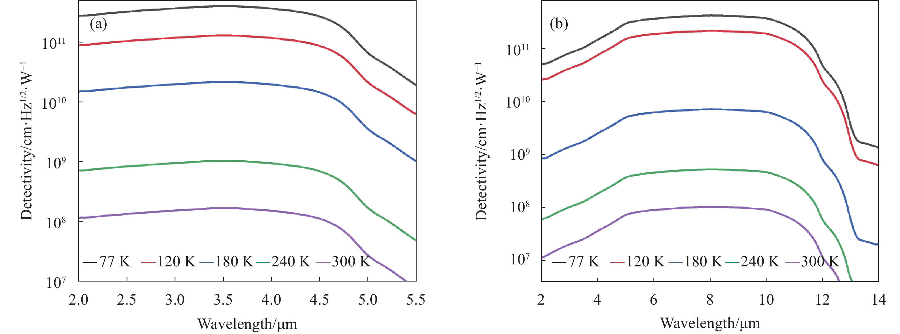
$$ \begin{split} {D^*} = {R_i}{\left[2qJ + \frac{{4kT}}{{{R_0}A}}\right]^{ - 1/2}} \end{split}$$ (11) 式中:Ri为响应度;J为器件的暗电流密度;T为器件的温度;R0为器件在零偏压下的电阻;A为器件的面积。计算得到的中波通道和长波通道的探测率如图9所示。在77 K下,中、长波峰值探测率为3.9×10¹¹、4.1×1011 cm·Hz1/2·W−1。

图 8 (a) 不同偏压下的中波与长波通道的光响应率;(b) 不同偏压下的中波与长波通道的量子效率
Figure 8. (a) Photoresponse simulations under different voltages; (b) Quantum efficiency simulations under different voltages
图 9 (a) 不同温度下的中波通道探测率;(b) 不同温度下的长波通道探测率
Figure 9. (a) Detectivity simulations of MWIR at different temperatures; (b) Detectivity simulations of LWIR at different temperatures
-
文中通过对nBn型的二类超晶格中/长波双波段探测器结构进行建模仿真,优化了吸收层和势垒层的厚度、掺杂浓度等来减小器件的暗电流和中波通道与长波通道间的串扰,得到了器件结构的各个参数,仿真得到了中波通道截止波长为4.8 µm (50%),在77 K下,外加0.3 V偏压时,暗电流密度为4×10⁻⁵ A·cm−2,RA为6.7×10³ Ω·cm2,峰值量子效率为64%,峰值探测率3.9×1011 cm·Hz1/2·W−1;长波通道截止波长为10.5 µm(50%),在77 K下,外加−0.3 V偏压时,暗电流密度为1.3×10⁻⁴ A·cm−2,RA为2.3×10³ Ω·cm2,峰值量子效率η为48%,峰值探测率4.1×1011 cm·Hz1/2·W−1,为后续材料生长和器件工艺提供了理论依据。从仿真方面证实了,基于15 MLs InAs/8 MLs GaSb和8 MLs InAs/6 MLs GaSb的nBn结构的中/长波双波段红外探测器是可行的。
文中设计的双波段探测器件具有器件结构简单和暗电流密度低等优点,性能方面与国外基于nBn结构的InAs/InAsSb红外探测器和国内基于PπMN结构的InAs/GaSb红外探测器等同类型器件相比,中波通道探测率相近,但长波通道探测率更高。仿真会与实际的器件性能结果有一定的差别,因此后续将会进行材料生长与器件工艺来进一步反馈仿真,同时在器件结构方面将会做进一步的改进。
Optimization of nBn dual-band mid-/long-wavelength detector based on InAs/GaSb superlattice
-
摘要: 双波段红外探测可对复杂的红外背景进行抑制,在军用目标识别、医疗诊断和污染监测等方面有重要应用价值。基于二类超晶格的双波段红外探测器在成本和性能方面具有很大的优势,成为新型红外探测器领域的研究热点。然而其暗电流和串扰会极大地影响双波段红外探测器的性能。因此,设计了nBn结构的InAs/GaSb超晶格中/长波双波段红外探测器,通过仿真比较不同结构的器件在不同偏压下的中波/长波通道的响应率和暗电流大小,分析势垒层厚度、吸收层厚度、不同区域的掺杂对暗电流和串扰的影响,从而得到最佳的模型参数达到减小暗电流和降低串扰的效果。仿真结果显示:nBn结构的中/长波双波段红外探测器在77 K下,中波通道的暗电流密度为4.5×10⁻⁵ A·cm−2,在0.3 V偏压下,2 µm处的峰值量子效率为64%,探测率可以达到3.9×1011 cm·Hz1/2·W−1;长波通道的暗电流密度为1.3×10−4 A·cm−2,在−0.3 V的偏压下,5.6 µm处的峰值量子效率为48%,探测率可以达到4.1×1011 cm·Hz1/2·W−1。相关结论可为器件设计和加工提供参考。
-
关键词:
- 红外探测器 /
- 双波段 /
- nBn /
- InAs/GaSb超晶格 /
- 暗电流
Abstract:Objective Infrared photodetectors are useful for a variety of military and civil applications, such as space science, military equipment, industrial production and so on. Presently, infrared photodetectors are developing towards high performance and low cost to meet the technical requirements. Compared to single color detectors, dual-band infrared detectors covering different atmospheric windows allow for simultaneous acquisition of target information in both wavelengths which is the most obvious advantage. Therefore, the dual-band capability of the detector makes it possible to discriminate between different temperatures and objects, improving the accuracy of temperature measurement and target recognition. Complex infrared backgrounds can be suppressed and it is possible to reduce the false alarm rates significantly in early warning, searching and tracking systems. Mid-long wavelength dual-band infrared detectors based on type II superlattice have great advantages in terms of cost and performance, and have become a popular research topic in the field of new infrared detectors. However, infrared detectors need to reduce dark current density and crosstalk to achieve better performance. The nBn superlattice detector has a unique band gap engineering approach, which can work at a higher temperature and has better thermal stability compared to traditional single color detectors. This leads to better performance and longer operating life in harsh environments. Additionally, the nBn structure has a high absorption coefficient, resulting in a high detectivity and low noise. However, the development of nBn superlattice dual-band detectors faces several challenges, such as the difficulties in fabrication and the limitations in performance. The fabrication of the nBn structure requires precise control of the layer thickness and doping levels, which is a complex process. Besides, the performance of the nBn detector is limited by dark current and temperature. These issues need to be addressed through further research and development. To this end, the paper designs an InAs/GaSb superlattice mid/long dual-band infrared detector with nBn structure to reduce dark current density and crosstalk by simulation of silvaco. Methods The materials of the mid-band and the long-band absorber are selected by calculating the band gap of InAs/GaSb using the k.p model to meet the requirements of the design objectives. The mid/long dual-band infrared detectors model with nBn structure is eatablished by silvaco, and the responsivity and dark current density values of the mid/long waveband channels are compared by simulating some device structures at different bias voltages. The effects of the barrier layer thickness, absorber layer thickness, and doping in different regions are analyzed to obtain the best model parameters to reduce the dark current density and crosstalk. Results and Discussions By modeling and simulating the nBn type II superlattice mid/long dual-band infrared detector structure, the thickness of the absorber and barrier layers and the doping concentration are optimized to reduce the dark current and the crosstalk in the mid-band and the long-band channel. At 77 K, the cutoff wavelengths of the dual-band detector are 4.8 µm (50%) at 0.3 V and 10.5 µm (50%) at −0.3 V (Tab.8) with the detectivies of 3.9×1011 cm·Hz1/2W−1 and 4.1×1011 cm·Hz1/2W−1 (Tab.9). The dark current density is 4×10⁻⁵ A·cm−2 and 1.3×10⁻⁴ A·cm−2 respectively (Tab.7). This provides a theoretical basis for subsequent material growth and device processes. Conclusions The advantages of the designed superlattice mid/long dual-band infrared detector are simple device structure, low dark current density, and similar detection rate compared with the foreign InAs/InAsSb infrared detectors based on nBn structure and domestic InAs/GaSb infrared detectors based on PπMN structure. The simulation performance will have some differences with the actual device performance, so the subsequent material growth and device process will be carried out to further feedback the simulation, and the device structure will be further improved. -
Key words:
- infrared detector /
- dual-band /
- nBn /
- InAs/GaSb superlattice /
- dark current
-
图 2 (a) 15 MLs InAs/8 MLs GaSb长波超晶格的能带图;(b) 8 MLs InAs/6 MLs GaSb中波超晶格的能带图;(c)中/长波双波段红外探测器结构
Figure 2. (a) Simulated band diagram of the 15 MLs InAs/8 MLs GaSb long-wave superlattices; (b) Simulated band diagram of the 8 MLs InAs/6 MLs GaSb mid-wave superlattices; (c) Mid/long wave dual-band infrared detector structure
图 3 (a) 不同Al组分的AlxGa1−xSb的能带图;(b)器件整体的能带图
Figure 3. (a) Simulated band diagram of the AlxGa1−xSb with different Al components; (b) Simulated band diagram of the device
图 4 (a) 77 K下不同势垒层厚度下的J-V曲线;(b) ±0.3 V下不同势垒层厚度下的光响应谱
Figure 4. (a) J-V curve under different thickness of barrier at 77 K;(b) Photoresponse simulations with different thickness of barrier at ±0.3 V
图 5 (a) 吸收层在不同掺杂浓度下的暗电流密度;(b) 吸收层在不同掺杂浓度下的光响应;(c) 势垒层在不同掺杂浓度下的暗电流密度;(d) 势垒层在不同掺杂浓度下的光响应;(e) 势垒层在不同掺杂浓度下的能带图
Figure 5. (a) Dark current density simulations of absorber with different doping; (b) Photoresponse simulations of absorber with different doping; (c) Dark current simulations of absorber with different doping; (d) Photoresponse simulations of absorber with different doping; (e) Simulated band diagram of absorber with different doping concentrations
图 6 (a) 不同中波吸收层厚度下的光响应率;(b) 不同长波吸收层厚度下的光响应率;(c) 不同中波吸收层厚度下的串扰;(d) 不同长波吸收层厚度下的串扰
Figure 6. (a) Photoresponse simulations with different thickness of mid-wave absorber; (b) Photoresponse simulations with different thickness of long-wave absorber; (c) Cross talk simulations with different thickness of mid-wave absorber; (d) Cross talk simulations with different thickness of long-wave absorber
图 7 (a) 不同温度下的J-V曲线;(b) 不同温度下的暗电流主导机制
Figure 7. (a) J-V curve under different temperatures; (b) Dark current dominant mechanism at different temperatures
图 8 (a) 不同偏压下的中波与长波通道的光响应率;(b) 不同偏压下的中波与长波通道的量子效率
Figure 8. (a) Photoresponse simulations under different voltages; (b) Quantum efficiency simulations under different voltages
图 9 (a) 不同温度下的中波通道探测率;(b) 不同温度下的长波通道探测率
Figure 9. (a) Detectivity simulations of MWIR at different temperatures; (b) Detectivity simulations of LWIR at different temperatures
表 1 15 MLs InAs/8 MLs GaSb 超晶格材料参数等效定义
Table 1. Material parameters of 15 InAs/8 GaSb superlattice
Parameter Value Electron effective mass (x m0) 0.024 Hole effective mass (x m0) 0.104 Permittivity/F.m−1 14.985 Electron affinity/eV 4.8179 Bandgap at 300 K/eV 0.12 Electron mobility at 300 K/cm2·V−1·s−1 1000 Hole mobility at 300 K/cm2·V−1·s−1 270  下载: 导出CSV
表 2 8 MLs InAs/6 MLs GaSb 超晶格材料参数等效定义
Table 2. Material parameters of 8 InAs/6 GaSb superlattice
Parameter Value Electron effective mass (x m0) 0.04 Hole effective mass (x m0) 0.75 Permittivity/F.m−1 15.3 Electron affinity/eV 4.667 Bandgap at 300 K/eV 0.258 Electron mobility at 300 K/cm2·V−1·s−1 1000 Hole mobility at 300 K/cm2·V−1·s−1 500
下载: 导出CSV
-
[1] He M, Xu Z, Zhang S W, et al. Colloidal InSb quantum dots/organic integrated bulk heterojunction for fast and sensitive near‐infrared photodetectors [J]. Advanced Photonics Research, 2022, 3(4): 2100305. doi: 10.1002/adpr.202100305 [2] Luo L, Huang Y, Cheng K, et al. MXene-GaN van der Waals metal-semiconductor junctions for high performance multiple quantum well photodetectors [J]. Light: Science & Applications, 2021, 10(1): 177. [3] Akhavan N D, Umana-membreno G A, Gu R, et al. Design principles for high QE HgCdTe infrared photodetectors for eSWIR applications [J]. Journal of Electronic Materials, 2022, 51(9): 4742-4751. doi: 10.1007/s11664-022-09809-y [4] Gawron W, Sobieski J, Manyk T, et al. MOCVD grown HgCdTe heterostructures for medium wave infrared detectors [J]. Coatings, 2021, 11(5): 611. doi: 10.3390/coatings11050611 [5] Hao H, Wang G, Xiang W, et al. Fabrication of type-II InAs/GaSb superlattice long-wavelength infrared focal plane arrays [J]. Infrared Physics & Technology, 2015, 72: 276-280. [6] Razeghi M, Dehzangi A, Li J. Multi-band SWIR-MWIR-LWIR Type-II superlattice based infrared photodetector [J]. Results in Optics, 2021, 2: 100054. doi: 10.1016/j.rio.2021.100054 [7] Ma X L, Guo J, Hao R T, et al. Growth and photo-electronic characteristics of short/mid wave dual-band infrared detectors based on GaSb bulk and InAs/GaSb superlattices [J]. Optical Materials Express, 2021, 11(2): 585-591. doi: 10.1364/OME.416272 [8] Rehm R, Walther M, Schmitz J, et al. Dual-colour thermal imaging with InAs/GaSb superlattices in mid-wavelength infrared spectral range [J]. Electronics Letters, 2006, 42(10): 1. [9] Hao X, Teng Y, Zhao Y, et al. Demonstration of a dual-band InAs/GaSb type-II superlattice infrared detector based on a single heterojunction diode [J]. IEEE Journal of Quantum Electronics, 2019, 56(2): 1-6. [10] Plis E, Myers S, Ramirez D, et al. Dual color longwave InAs/GaSb type-II strained layer superlattice detectors [J]. Infrared Physics & Technology, 2015, 70: 93-98. [11] Zhu Xubo, Peng Zhenyu, Cao Xiancun, et al. Mid-/short-wavelength dual-color infrared focal plane arrays based on type-II InAs/GaSb superlattice [J]. Infrared and Laser Engineering, 2019, 48(11): 1104001. (in Chinese) [12] Rogalski A. Dual-band infrared detectors [J]. Journal of Infrared and Millimeter Waves, 2000, 19(4): 241-258. [13] Plis E, Krishna S S, Smith E P, et al. Voltage controllable dual-band response from InAs/GaSb strained layer superlattice detectors with nBn design [J]. Electronics Letters, 2011, 47(2): 133-134. doi: 10.1049/el.2010.3096 [14] Hoang A M, Chen G, Haddadi A, et al. High performance bias-selectable dual-band short-/mid-wavelength infrared photodetectors based on type-II InAs/GaSb/AlSb superlattices [J]. Applied Physics Letters, 2013, 102(1): 11108. [15] Haddadi A, Chevallier R, Chen G, et al. Bias-selectable dual-band mid-/long-wavelength infrared photodetectors based on InAs/InAs1−xSbx type-II superlattices [J]. Applied Physics Letters, 2015, 106(1): 011104. doi: 10.1063/1.4905565 [16] 孙姚耀, 韩玺, 吕粤希, 等. 基InAs/GaSb二类超晶格的中/长波双色红外探测器[J]. 航空兵器, 2018, 4(02): 56-59. Sun Yaoyao, Han Xi, Lv Yuexi, et al. Performance of dual-color mid-/long-wavelength infrared detectors based on type-II InAs/GaSb superlattice [J]. Aero Weaponry, 2018, 4(2): 56-59. (in Chinese) [17] 朱旭波, 彭震宇, 曹先存, 等. InAs/GaSb二类超晶格中/短波双色红外焦平面探测器[J]. 红外与激光工程, 2019, 48(11): 1104001-1104001(6). doi: 10.3788/IRLA201948.1104001 Zhu Xubo, Peng Chenyu, Cao Xiancun, et al. Mid-/short-wavelength dual-color infrared focal plane arrays based on type-II InAs/GaSb superlattice [J]. Infrared and Laser Engineering, 2019, 48(11): 1104001. (in Chinese) doi: 10.3788/IRLA201948.1104001 [18] 李俊斌, 刘爱民, 蒋志, 等. InAs/GaSb超晶格长波红外探测器暗电流特性分析[J]. 红外与激光工程, 2022, 51(4): 20210399. doi: 10.3788/IRLA20210399 Li Junbin, Liu Aimin, Jiang Zhi, et al. Analysis of dark current characteristic of InAs/GaSb superlattice longwave infrared detectors [J]. Infrared and Laser Engineering, 2022, 51(4): 20210399. (in Chinese) doi: 10.3788/IRLA20210399 [19] Callewaert F, Hoang A M, Razeghi M. Generation-recombination and trap-assisted tunneling in long wavelength infrared minority electron unipolar photodetectors based on InAs/GaSb superlattice [J]. Applied Physics Letters, 2014, 104(5): 053508. doi: 10.1063/1.4864403 [20] Alchaar R, Rodriguez J B, Hglund L, et al. Characterization of an InAs/GaSb type-II superlattice barrier photodetector operating in the LWIR domain [J]. AIP Advances, 2019, 9(5): 055012. doi: 10.1063/1.5094703 [21] Rogalski A. Infrared detectors: status and trends [J]. Progress in Quantum Electronics, 2003, 27(2-3): 59-210. doi: 10.1016/S0079-6727(02)00024-1 [22] Qiao P F, Mou S, Chuang S L. Electronic band structures and optical properties of type-II superlattice photodetectors with interfacial effect [J]. Optics Express, 2012, 20(3): 2319-2334. doi: 10.1364/OE.20.002319 [23] Steveler E, Verdun M, Portier B, et al. Optical index measurement of InAs/GaSb type-II superlattice for mid-infrared photodetection at cryogenic temperatures [J]. Applied Physics Letters, 2014, 105(14): 141103. doi: 10.1063/1.4897273 [24] Delmas M, Rodriguez J B, Christol P. Electrical modeling of InAs/GaSb superlattice mid-wavelength infrared pin photodiode to analyze experimental dark current characteristics [J]. Journal of Applied Physics, 2014, 116(11): 113101. doi: 10.1063/1.4895983 [25] 赵俊, 毛京湘, 李艳辉, 等. 双色焦平面红外探测器相对光谱串音研究[J]. 红外技术, 2014, 36(4): 286. Zhao Jun, Mao Jingxiang, Li Yanhui, et al. Analysis on the relative spectral crosstalk of dual-band IRFPA detector [J]. Infrared Technology, 2014, 36(4): 286. (in Chinese) -

 点击查看大图

计量
- 文章访问数: 165
- HTML全文浏览量: 49
- PDF下载量: 79
- 被引次数: 0

