


-
工作在通讯波段1310 nm和1550 nm波段的短波红外单光子探测器(SPAD),在光纤通讯、激光雷达、量子保密通讯等技术领域具有广泛的应用需求。结合对人眼安全的应用考虑,1550 nm短波红外单光子探测器体现出了更为广泛的应用,同时也对高探测效率、高计数率、高温工作、低成本的单光子探测器提出了迫切的发展需求。
随着InP/InGaAs短波红外单光子探测器(SPAD)在材料结构、材料质量、工艺制备和淬灭电路等方面的不断改进和发展,目前InP/InGaAs SPAD的性能获得了显著的提升,探测效率典型值从20%提升到30%,而暗计数率进一步降低,低于kHz[1]。另外一个显著的性能提升是用以抑制器件后脉冲的死时间降低,通过优化淬灭电路、采用负反馈单光子探测器等方法,目前报道的死时间已经从μm量级提升到亚μs[2]。这对于高速应用提供了重要的芯片技术支撑。
对于1550 nm的单光子探测技术,除了传统的InP/InGaAs SPAD,目前还发展了Sb基数字合金构建的低噪声材料体系、采用离化工程的多倍增InP/InGaAs SPAD、InAlAs/InGaAs SPAD等新材料、新结构探测技术,使短波红外单光子探测芯片技术获得了快速的发展和进步。
文中对近10年来基于InP/InGaAs SPAD的技术改进进行了归纳总结,分析了器件设计和研制中面临的主要问题、技术解决途径和取得的进展,重点介绍了国内外高温、高速InP/InGaAs单光子探测器及焦平面阵列的发展,对探测效率、暗计数率、后脉冲和时间抖动等性能进行了对比分析;最后结合出现的离化工程、新机理新材料体系,探讨了短波红外单光子探测器未来的发展趋势。
-
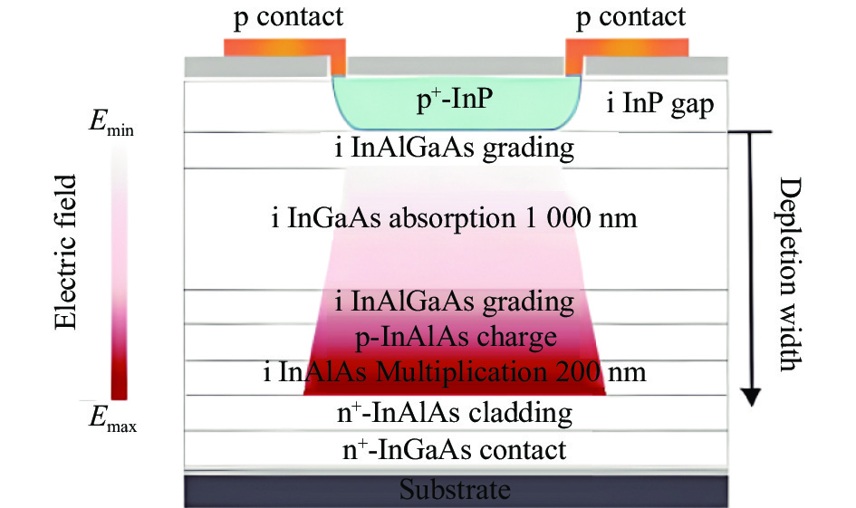
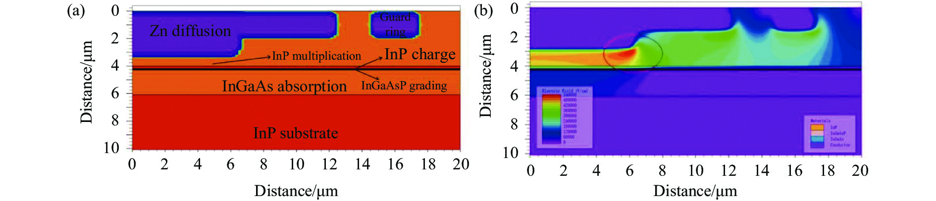
InP和In0.53Ga0.47As材料晶格匹配,但具有不同的带隙值,室温下两者的禁带宽度分别约为1.35 eV和0.75 eV,因此,采用这两个材料作为倍增层和吸收层,一方面对应着截止波长1.65 μm的吸收,另外一方面宽带隙InP倍增层可大大降低高电场下的隧穿电流。因此,分离吸收、渐变、电荷、倍增(即:separate absorption, grading, charge, and multiplication, SAGCM)结构一旦被发明和应用以来,一直沿用至今,如图1(a)所示,入射光在InGaAs吸收区中被吸收形成电子空穴对,在电场作用下光生电子空穴对被分开,空穴经过渐变层及电荷层漂移到InP倍增区。在倍增层中空穴与晶格碰撞产生新的电子空穴对,新的电子空穴对在电场中加速与晶格碰撞产生新的电子空穴对,该过程重复发生,载流子触发自持雪崩,使微弱的光信号转化为足以探测的电信号。结构中渐变层消除了InGaAs-InP异质界面处的空穴堆积;薄且高掺杂的电荷层调控了吸收区和倍增区的电场,使SPAD在工作时吸收区电场足够低以避免载流子遂穿,同时倍增区的电场足够高以确保载流子在倍增区能触发雪崩倍增,通过保护环降低边缘击穿。

图 1 (a) InP/InGaAs SPAD结构示意图;(b) 击穿时SPAD内部电场分布
Figure 1. (a) Schematic diagram of InP/InGaAs SPAD; (b) Electric field distribution inside SPAD at breakdown voltage
InP/InGaAs SPAD设计的重点在于精确控制吸收区、倍增区的电场大小。根据InP、InGaAs材料的禁带宽度,为了避免发生带间隧穿,要求在两种材料内的电场不能高于7×10⁵ V/cm,1.5×105 V/cm,而为了维持载流子在倍增区的雪崩和在吸收区的漂移,两种材料内最低的电场需要大于4.5×105 V/cm,1.0×105 V/cm。为此需要优化设计电荷层、倍增层等材料参数,同时要求材料生长时能精确控制各层的掺杂浓度和厚度。
倍增区内的电场分布不均匀,尤其边缘尖峰电场会引入过早的边缘击穿,使器件无法正常雪崩,器件性能大大衰退。因此实际器件制备时通常要采用二次扩散和增加保护环来抑制边缘击穿,但器件内部仍存在不均匀电场,如图1(b)所示,图中给出了器件处于击穿电压下的电场的二维分布,其中的红圈位置是由于二次扩散时形成的尖角产生的不均匀区域,该区域内电场高于中心倍增区内的电场,导致过早的边缘击穿和大的暗计数。因此实现均匀的雪崩电场也是InP/InGaAs SPAD设计和制备的一个重点。
针对以上两个关键问题,为了精确控制电场大小,并获得均匀的倍增区电场分布,目前主要采用以下几种方法:(1)使用以二甲基锌作为锌源的金属有机化学气相沉积(MOCVD)设备进行锌扩散,通过调整扩散参数包括Zn 扩散温度、磷化氢超压和二甲基锌源流速等,优化电场分布和倍增区的缺陷分布。(2)采用两步同心扩散方法控制二极管中心区域的p-n结比外部区域更深。(3)在器件的中心处选择性生长未掺杂的锥形InP层,获得中心区薄、而边缘逐渐增厚的InP层,通过这一锥形InP层扩散锌,使InP中心区的掺杂比外围区更深,从而确保器件中心区电场高于边缘周围的电场。(4)增加电荷层浓度,在InGaAs吸收区中实现较低的电场,以减少来自吸收层场增强产生的暗计数率。
目前InP/InGaAs SPAD还存在着的一个问题是后脉冲现象,这也是当前制约InP/InGaAs在高速应用中的一个瓶颈问题。这主要是由于InP倍增层里存在深能级缺陷,对倍增层里产生的大量雪崩载流子进行俘获,并慢慢释放导致虚假雪崩计数信号,后脉冲会增加暗计数,产生误计数。为了降低后脉冲概率,目前采用的主要方法有:(1)对InP材料生长技术和SPAD芯片工艺的持续改进;(2)适度降低雪崩载流子数,但这同时降低了探测效率;(3)通过增加两次雪崩之间的时间(又称之为死时间),使陷阱俘获的载流子获得充分的释放,从而降低后脉冲概率,但这大大降低了最大计数率。(4)通过采用正弦门控的淬灭方式,减少雪崩时的门宽时间,降低雪崩量,从而减小后脉冲。
-
通过对器件结构参数的优化设计,在器件光入射窗口涂上抗反射涂层或增加微透镜,优化器件制备工艺条件使有源区电场更均匀,大大改善了InP/InGaAs SPAD的探测效率、降低了暗计数率,近10年国内外有代表性的进展如表1所示。
表 1 近10年报道的高探测效率InP/InGaAs SPAD的性能汇总
Table 1. Summary of the InP/InGaAs SPADs with high detection efficiency reported in the past decade
Institution Year Detection efficiency Temperature/K Dark count rate/kHz Time jitter/ps Afterpulse probability Politecnico di Milano 2012[3] >25% 225 100 <90 - 2014[4] 28% 225 few 87 - 2021[5] 11%-30% 225 1.46-6.47 340-119 1%-5.9% University of Science
and Technology of China2020[6] 40% 253 14.5 - 5.5% 2022[1] 30% 233 0.665 - About 15% Institute of Semiconductors,
Chinese Academy of Sciences2022[7] 25.72% 223 9.09 - - Princeton Lightwave 2014[8] 25% 225 6 - - 2020[9] >10% 233 <10 - <10% Chongqing Institute of
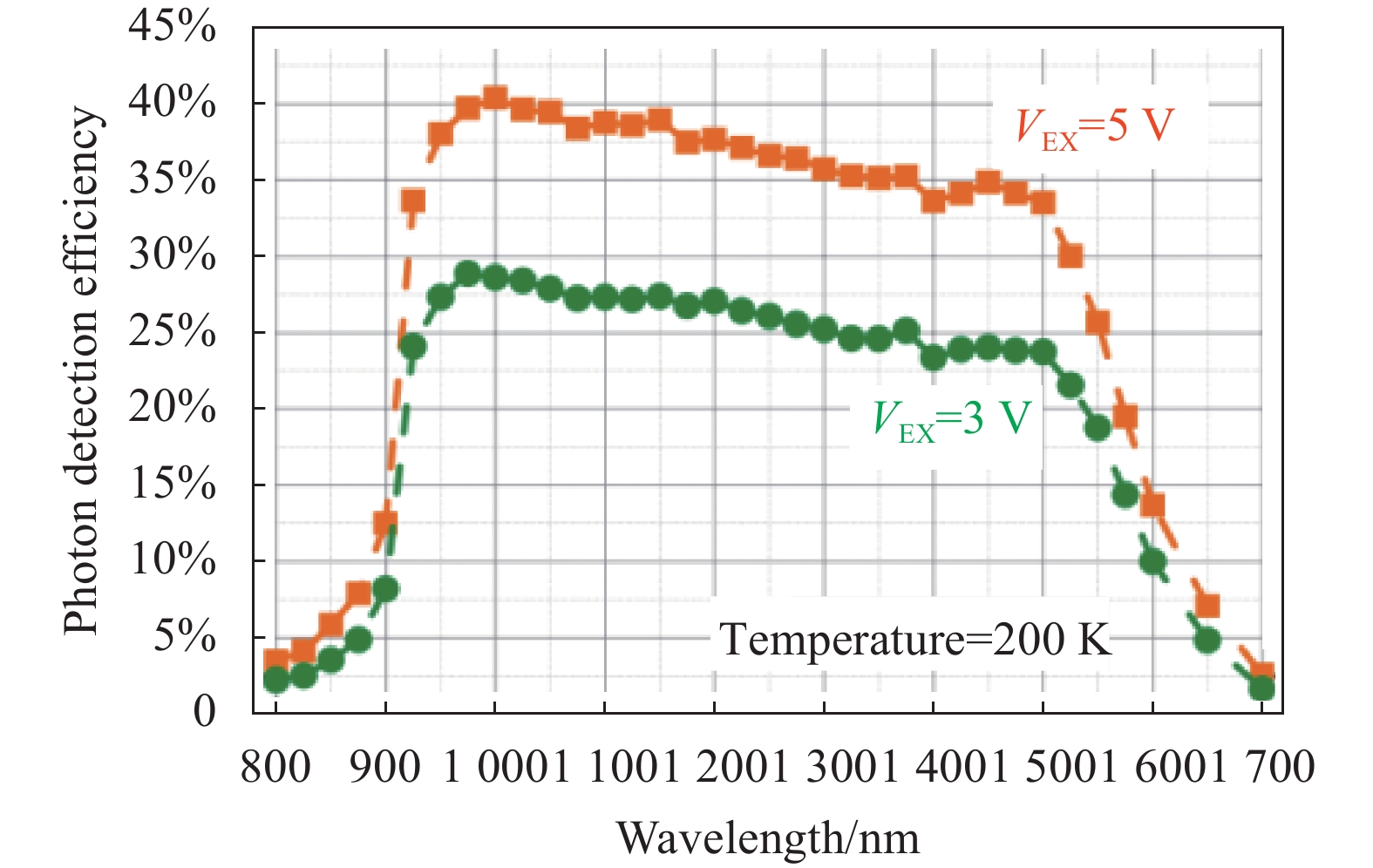
Optoelectronic Technology2017[10] 20% 223 1 - - Yunnan University 2022[11] 35.7% 233 3.3 - - 探测效率是光电探测器的重要指标,表征了器件的光电探测能力。该效率是几个效率的乘积,包括量子效率、空穴被注入到倍增区的概率、空穴在倍增层触发雪崩的概率、雪崩被探测到的概率,因此,提高器件的量子效率可提高探测效率。2012年,米兰理工大学[3]报道了在原有的SAGCM结构顶部加上针对1550 nm光子优化的200 nm SiNx抗反射涂层,以减少光子的反射,提高量子效率。该SPAD在5 V过偏压下,200 K时,不同波长的光与探测效率关系如图2所示,对于1550 nm波长的光探测效率>25%,对于1000 nm的光探测效率为40%。

2020年,中国科学技术大学[6]制备了平面背入射式SPAD,通过增加介电-金属反射层,使入射光子的吸收效率相对提高20%。在1.25 GHz 正弦波门控和不同正弦门峰峰值条件下测试了暗计数率和探测效率随温度的变化关系,测试结果如图3(a)所示,其中门高峰峰值为10.5 V,工作温度为253 K时,SPAD的探测效率约40 %,暗计数率为 14.5 kHz (归一化)。

图 3 (a) 中国科学技术大学1.25 G正弦门控,不同温度、不同峰峰值条件下探测效率与暗计数的关系[6];(b) 中国科学技术大学金属层和三个周期的SiO2/TiO2布拉格反射镜组成的增强反射结构[1]
Figure 3. (a) Relationship between detection efficiency and dark counts rate under different temperatures and different peak-to-peak values with 1.25 G sinusoidal gating from University of Science and Technology of China[6]; (b) Enhanced reflection structure consisting of metal layer and three-cycle SiO2/TiO2 Bragg mirror made by University of Science and Technology of China[1]
2022年,中国科学技术大学[1]提出在p+掺杂InP接触层上增加由金属层和三个周期的SiO2/TiO2布拉格反射镜组成的增强反射结构,如图3(b)所示,同时采用了微透镜的结构,对12 μm有源区和1.1 μm吸收层厚度的SPAD吸收效率提高了58%。在233 K温度下,门控频率为50 MHz时,探测效率分别为10%、20%和30%,对应的归一化暗计数率分别为127 Hz、361 Hz和665 Hz。
暗计数率也是器件的一个重要性能指标,器件在工作时,希望探测效率高的同时暗计数尽可能低。暗计数率是器件在没有光照条件下,单位时间内器件内部触发雪崩的次数,是一个统计平均值,表征SPAD的基本噪声。暗计数主要来源于In0.53Ga0.47As窄带隙吸收区材料热激发及InP倍增层里的遂穿,为了减少由热激发带来的暗计数,将SPAD降温是一种有效的方法。暗计数的另一主要来源是倍增层里的隧穿,这主要是器件内部有源区高电场造成的,电场的不均匀、局部电场高也会引起场致隧穿或缺陷辅助隧穿,所以选择最佳的工艺条件使有源区电场更均匀,减少材料缺陷也是降低暗计数可行的方法。
2014年,米兰理工大学[4]报道了使用以二甲基锌作为锌源的金属有机化学气相沉积反应器扩散锌,通过改进锌扩散条件,获得均匀的雪崩电场,与之前的SPAD相比,提高了探测效率同时降低了器件噪声,实验结果如图4所示。有源区直径为25 μm的SPAD,对于1550 nm的光,在门控模式、5 V过偏压,温度为225 K时,探测效率为28%,暗计数率只有几kHz。

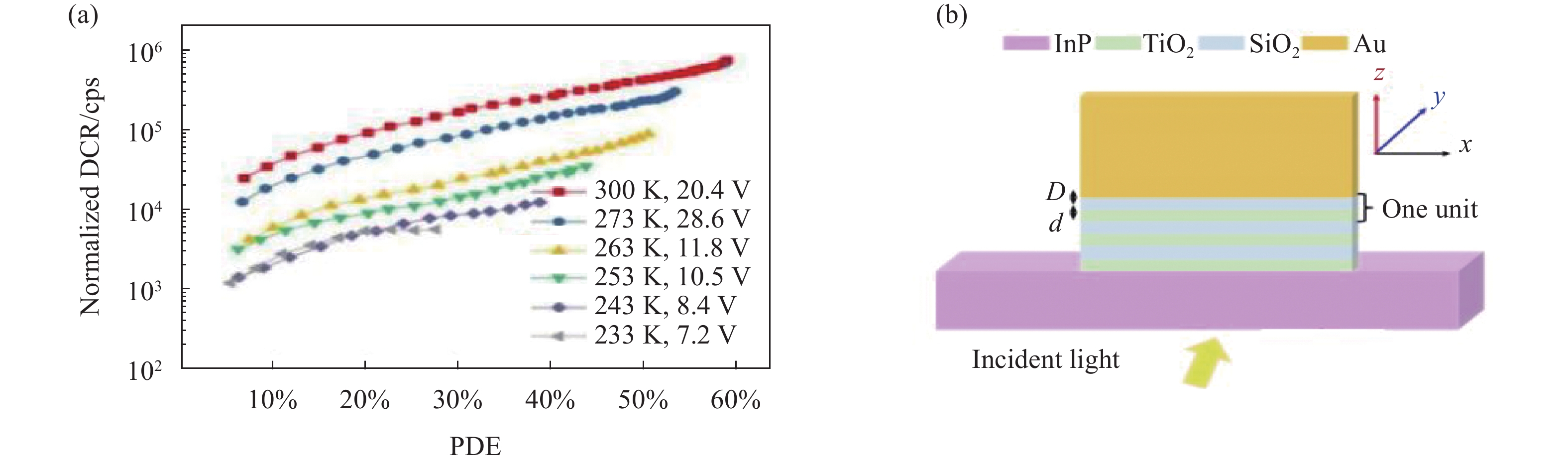
2021年,米兰理工大学[5]基于之前的实验数据及模拟数据,进一步优化改进器件结构,保持InP帽层厚度不变,而锌扩散深度较浅,使倍增区域较厚,击穿时具有较低电场,减少场增强载流子的产生;增加电荷层中的电荷,减少来自吸收区场增强产生的暗计数率,在InGaAs吸收区中实现较低的电场,整体改善雪崩二极管暗计数率。对于10、25 μm的InP/InGaAs SPAD, 5 V过偏压、温度为225 K时,在门控模式下暗计数率分别约为1、4 kHz;而10 μm的SPAD,在175 K温度下暗计数率降低到几十Hz。不同温度下暗计数率与过偏压的关系如图5所示。

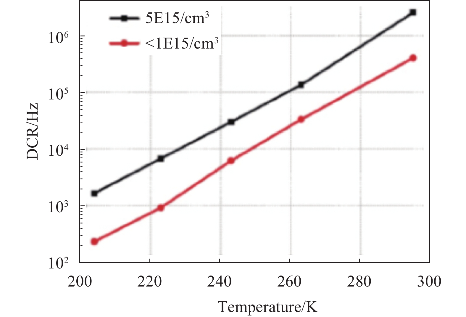
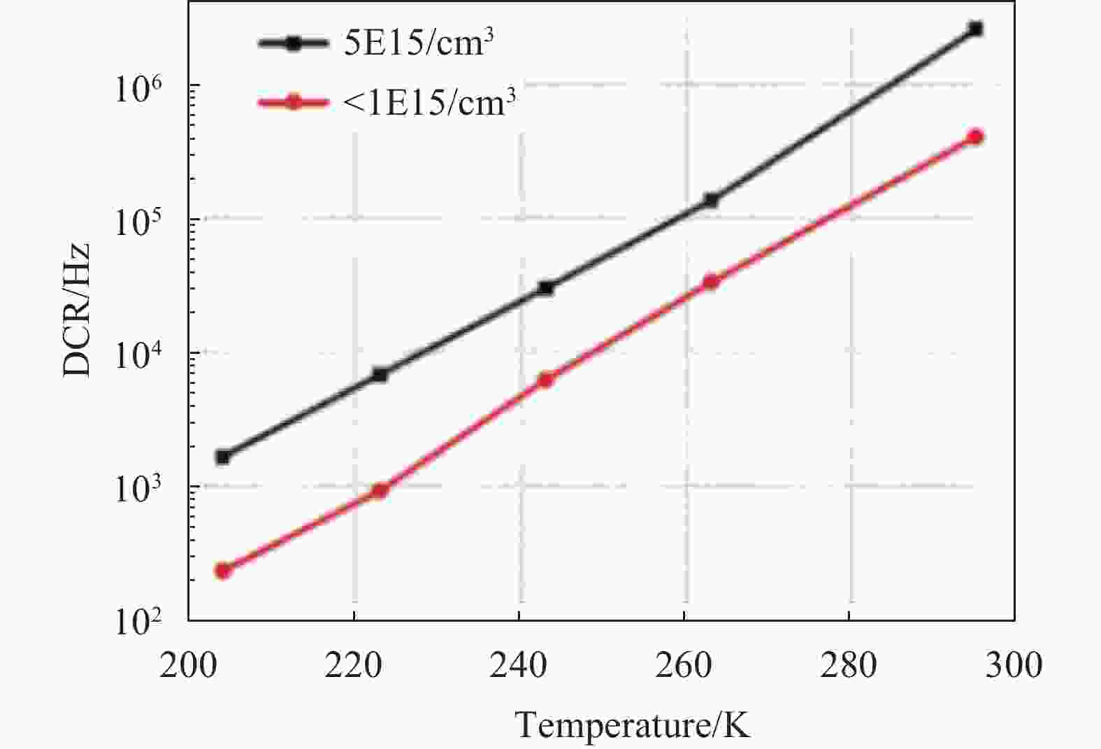
2017年,重庆光电技术研究所[10]基于InP顶层的掺杂浓度越低越有利于抑制边缘击穿,降低隧穿暗载流子的产生速率,提高雪崩击穿几率的理论计算结果,制造了InP顶层为非故意掺杂层的SPAD,在223 K下获得了20%的单光子探测效率和1 kHz的暗计数率,其探测效率比顶层掺杂浓度为5×10¹⁵/cm3的SPAD高3%~8%,而暗计数率低一个量级,两种设计的SPAD温度与暗计数的关系如图6所示。
2021年,云南大学[11]通过优化材料结构、材料质量和器件工艺,制备了有源区直径为12 μm的InP/InGaAs SPAD,通过电容平衡和双脉冲雪崩信号提取的门控淬灭方进行性能测试,门控频率为1 MHz,门高5 V,1550 nm激光的重复频率为500 kHz,每脉冲1个光子,工作温度233 K,测得探测效率为35.7%,暗计数率为3.3 kHz。
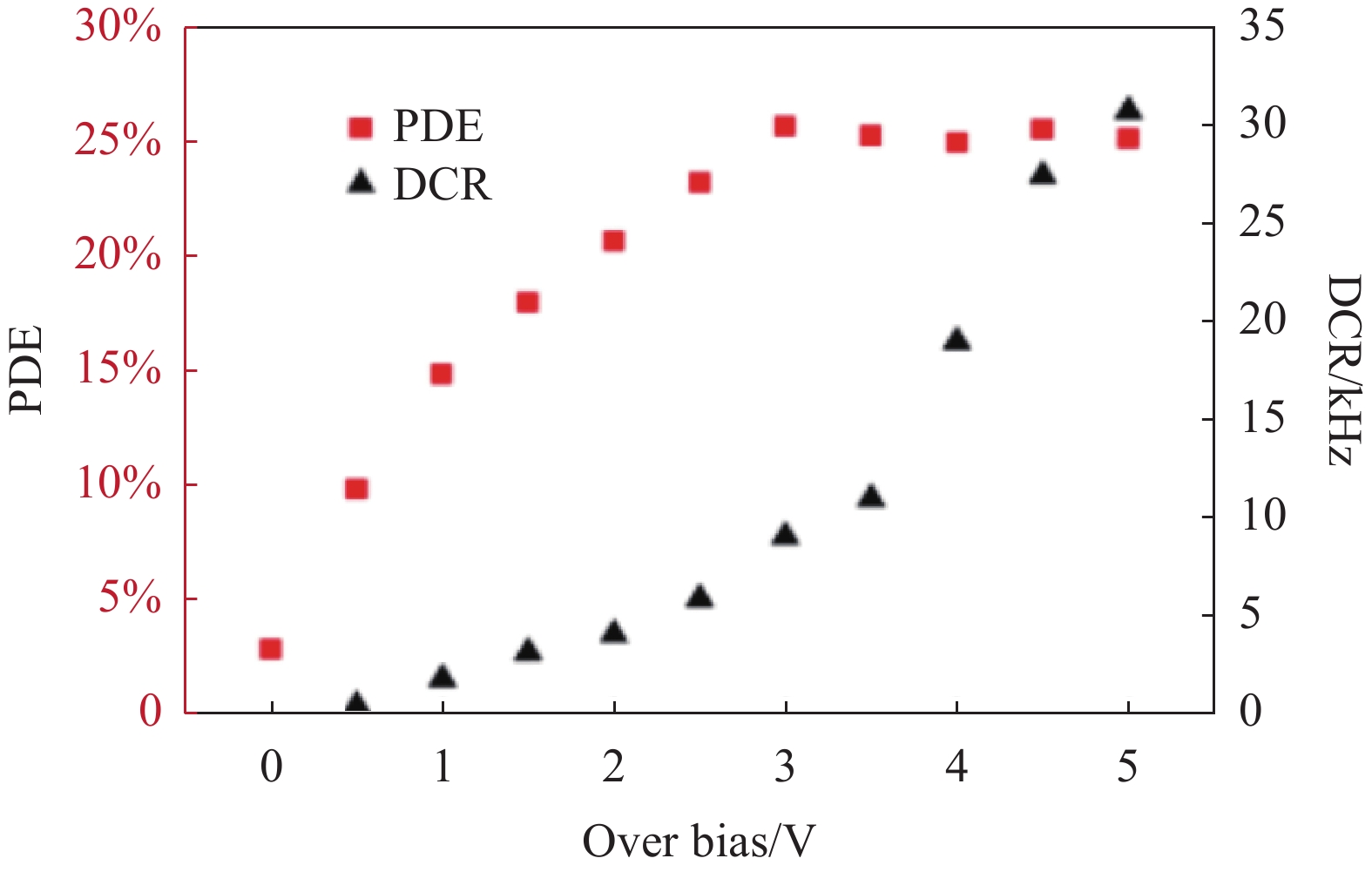
2022年,中国科学院半导体研究所[7]采用两步同心闭管扩散方法使二极管中心区域的p-n结比外部区域更深,制备了无保护环结构的SPAD。扩散时气压为5×10⁻⁴ Pa,扩散温度为550 ℃,两次扩散时间分别为30 min和8 min,器件中心和外围的p-n结深度分别为2.5 μm和1.8 μm。该有源区直径为25 μm的SPAD样品器件在门控模式下,探测效率、暗计数与过偏压的关系如图7所示,图中过偏压为3 V时,探测效率为25.72%,暗计数率为9.09 kHz。
-
InP/InGaAs SPAD需要在低温(约230 K)下工作,以降低暗计数率,但在低温时SPAD后脉冲大。若器件在室温条件下能保持可接受的暗计数率和探测效率,对抑制后脉冲、提高计数率具有显著的优势。工作温度为室温或接近室温(如零度以上,通过一级TEC很容易实现)被视为高温工作条件,有别于常规制冷单光子探测器,高温工作的单光子探测器需要对暗计数进行特别的抑制,一方面,这需要在材料结构、器件结构上进行特殊的设计,确保吸收区、倍增区与热有关的载流子激发、隧穿降至最小,由此引发的暗计数最小,暗计数率控制在可接受的范围内;另外一方面,通过运用正弦门控淬灭电路亚ns级的有效门宽,减少暗计数,也能使性能较好的单光子探测器在室温下工作。目前报道的高温器件性能如表2所示。
表 2 国内外报道的室温SPAD性能
Table 2. Performance of SPAD operating at room temperature
Institution Year Temperature/K Detection efficiency Dark count rate/kHz Afterpulse probability Time jitter/ps University of Shanghai for
Science and Technology2017[12] 293 21% 551 1.4% - Woorio Co Ltd 2021[13] 293 20.9% 5.1 0.8% - École Polytechnique
Fédérale de Lausanne2022[14] 300 43% 4000 - 109 National University of
Defense Technology2018[15] 294 10.6% 2.5×10⁻⁵/gate 1.3% - 2021年,韩国Wooiro公司[13]设计制备了有源区直径小、具有背面微透镜的InP/InGaAs SPAD,如图8所示,微透镜可以增强光线采集能力,在减小有源区直径的同时提高填充因子。该SPAD在门控频率为10 MHz,门高为6.6 V的门控模式下,对于1550 nm的光,在 293 K的工作温度下,测得探测效率为20.9%,暗计数率为5.1 kHz,后脉冲概率为0.8%。

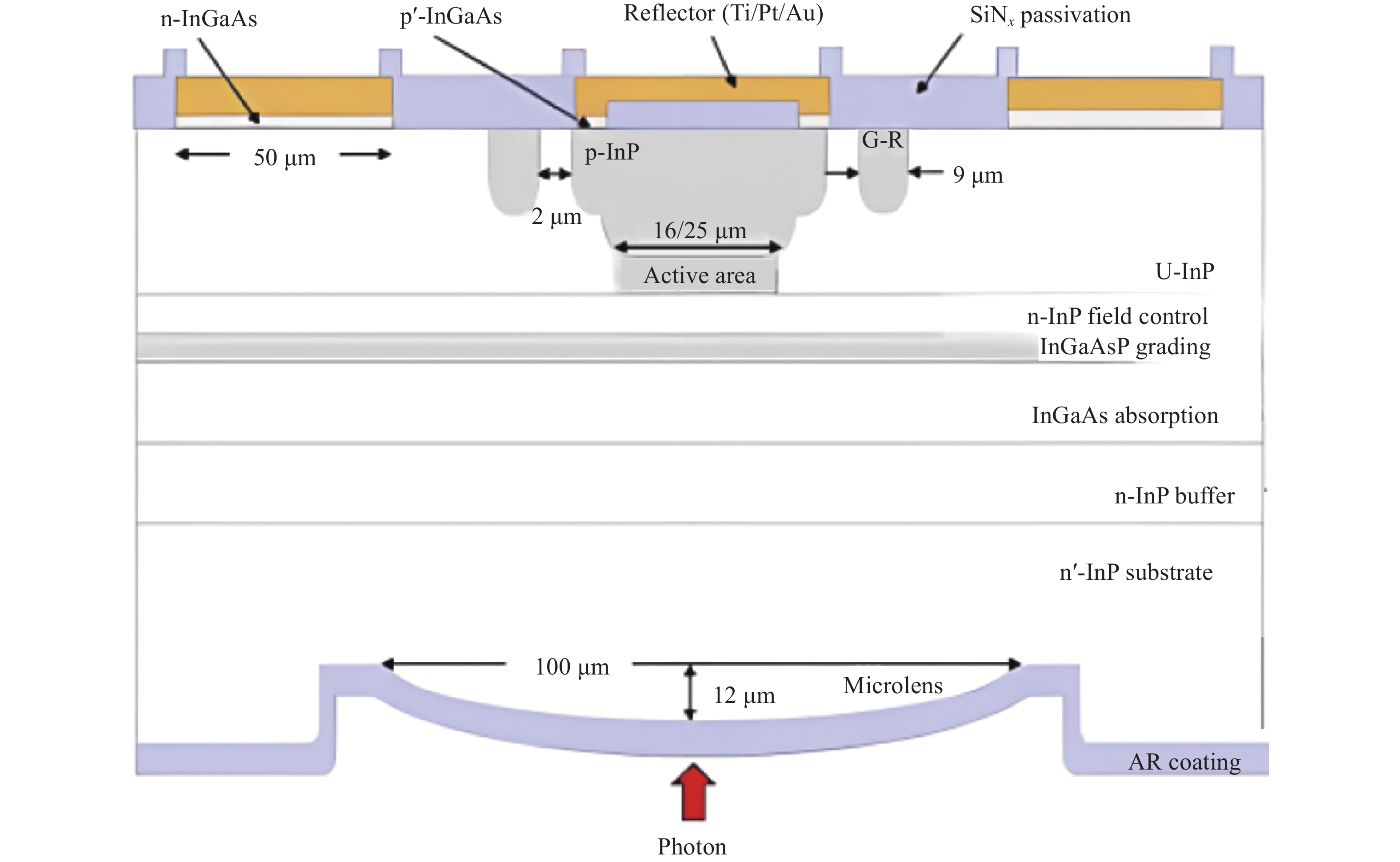
2022年,洛桑联邦理工学院[14]报道了Zn扩散之前,在器件的中心处选择性区域内生长约300 nm厚的未掺杂的锥形InP层。Zn扩散时通过锥形InP层,使InP内部的掺杂轮廓向外围稳定过渡,确保器件边缘周围的电场低于中心,SPAD截面图如图9所示。制成有源区直径为70 μm的SPAD,对于1550 nm的光,温度为300 K,过偏压为5 V时,探测效率为32%,暗计数率为1.6 MHz,时间抖动为149 ps;过偏压为7 V时,探测效率为43%,暗计数率为4 MHz,时间抖动为109 ps。

门控模式下采用正弦门,SPAD电容响应频率分布相对简单,主要集中在门的重复频率及其谐波频率上,采用低通滤波器很方便滤除噪声提取雪崩信号。2017年,上海理工大学[12]采用两个1.05 GHz截止的低通滤波器,其中一个在1.5 GHz频率下衰减高于40 dB,用于滤除尖峰噪声;另外一个用于提高射频放大器放大的雪崩信号信噪比。对于该设计电路,如果门控频率发生变化,则只需相应地更改带通滤波器,而无需更改用于消除尖峰噪声的组件。采用普林斯顿光波公司制造的SPAD(型号为PGA-300-1),对于1550 nm的光,温度为293 K,正弦门控频率为1.5 GHz,峰峰值为14 V,有效门宽为145 ps,探测效率为约21%,暗计数率为551 kHz (归一化),后脉冲概率为1.4%。
2018年,国防科技大学[15]报道了室温下门控频率可调(从900~1000 MHz)的取样电路研究工作。采用模数转换器将每个周期时钟内APD输出数字化,调整采样时钟与门控延时以确保每个周期内准确地采样。采用普林斯顿光波公司生产的InP/InGaAs SPAD,对于1550 nm的光,温度为294 K时,正弦门控频率为1 GHz,门宽未知的门控模式下,探测效率约10.6%,每门暗计数率为2.5×10⁻⁵,后脉冲概率为1.3%。
-
InP/InGaAs SPAD向高计数率发展面临的一个关键问题是死时间不断变短带来的后脉冲概率增大。通过采用正弦门、自差分等技术目前实现了GHz的高速SPAD,相关的性能指标如表3所示。
表 3 近10年报道的高计数率InP/InGaAs SPAD的性能汇总
Table 3. Summary of the InP/InGaAs SPADs with high count rate reported in the past decade
Institution Year Method Frequency/
GHzTemperature/
KDetection
efficiencyDark count rate/
kHzAfterpulse
probabilityNihon University 2020[16] Sine-wave gating 1.27 289 55.9% 2350 4.8% Toshiba Research Europe Ltd 2015[17] Self-
differencing1 293 55% - 10.2% University of Science and
Technology of China2020[6] Sine-wave gating 1.25 300 60.1% 744 14.8% ID Quantique 2019[18] Dual anode SPAD 1 253 20.4% 54.25 3.5% -
日本大学的Naoto Namekata等人在2006年最早报道将800 MHz高频正弦门控技术应用到InP/InGaAs SPAD中用作门控淬灭[19],从而开始了将高速门控InP/InGaAs SPAD最大计数率引领到GHz的水平。利用高频正弦门控亚纳秒量级门宽、超窄死时间,以及通过SPAD后输出信号纯净的频谱成分这三大特点,Naoto Namekata等人在输出端口利用带阻滤波器滤去正弦门控信号及其高次谐波,成功从约0.1 mV的背景噪声中提取到了振幅约1 mV的微弱雪崩信号。通过不断优化系统,他们在2009年报道了正弦门控技术实现门控频率达到2 GHz的InP/InGaAs SPAD[20],并于2011年[21]演示了超过100 km的量子密钥分发。在2020年[16],报道了过偏压超过12 V的高探测效率的正弦门控InP/InGaAs SPAD。在1.27 GHz门控频率下,55.9%探测效率时,后脉冲概率仅为4.8%,暗计数率为2350 kHz (归一化)。利用正弦门控技术,日内瓦大学于2010年[22]实现了迄今为止速度最快的InP/InGaAs SPAD,2.23 GHz的门控频率,已经逼近InP/InGaAs SPAD的理论带宽极限。
2020年,中国科学技术大学[6]在温度为300 K时,使用门高峰峰值为20.4 V,频率为1.25 GHz正弦门控,获得了探测效率为60%,暗计数率为744 kHz,和后脉冲概率为14.8%的结果。
-
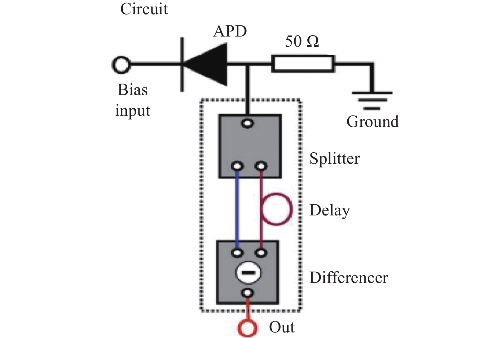
2007年,东芝欧洲研究有限公司[23]使用他们提出的自差分技术实现1.25 GHz方波门控(方波幅值4.6 V)下的高速InP/InGaAs SPAD,自差分电路如图10所示。该技术原理是首先将SPAD阳极输出的信号用功率分配器分割为两路,其中一路输出信号被延时一个周期,接着再直接将这两路输出信号进行差分,消除SPAD容性响应及电路寄生电容电感响应,雪崩信号即很容易地被提取。该技术的优点是可以采用多种延时手段、自差分原理可以适应任意SPAD输出信号的波形,但雪崩互相抵消的缺点导致自差分技术的最大理想计数率仅为门频率的一半。
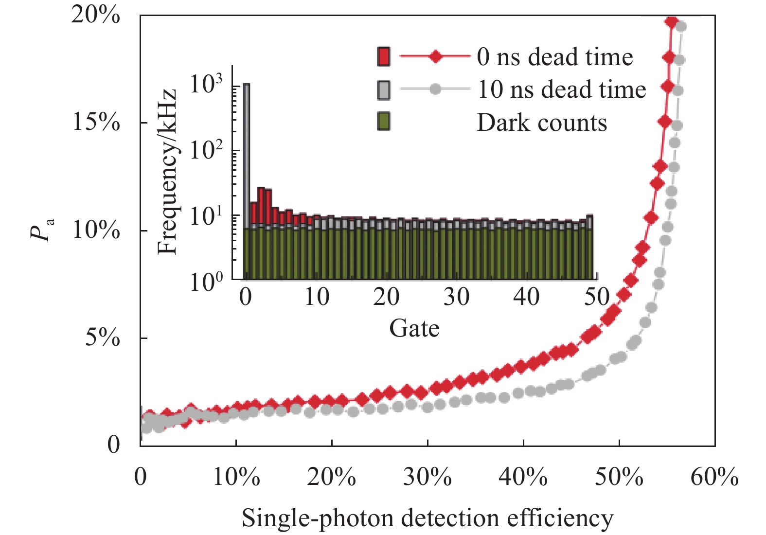
基于2007年报道的自差分电路技术,2015年东芝研究欧洲有限公司[17]优化了自差分模式,在该模式下使用频率为1 GHz,门宽为360 ps的门控信号,1550 nm的激光,温度为293 K,InP/InGaAs SPAD探测效率与后脉冲概率关系如图11所示。当探测效率为50%时,死时间为零时后脉冲概率为7%;当InP/InGaAs APD的探测效率为55%时,采集死时间为10 ns测量的后脉冲概率仅为10.2%。
-
焦平面阵列具有广泛应用,特别是人眼安全的1550 nm的InP/InGaAs SPAD阵列,可用于三维成像、激光雷达等。像素之间的串扰问题是制约高密度阵列性能的主要问题。另外,焦平面阵列的均匀性是保证焦平面工作的重要参数,阵列中像素的击穿电压越接近,其工作电压越接近,阵列工作条件实现越容易。阵列均匀性包括击穿电压均匀性、暗电流均匀性、探测效率均匀性、暗计数均匀性,通常通过阵列元素的击穿电压分布、暗电流分布、暗计数分布、探测效率分布进行表征,目前国内外均有研究团队对焦平面阵列性能进行了报道,相关性能比较见表4。
表 4 近10年SPAD焦平面阵列性能汇总
Table 4. Summary of SPAD focal plane array performance in the past ten years
Institution Year Format/
pixelPixels pitch/
µmTemperature/
KBreakdown voltage/
VDark current/
nAAverage detection
efficiencyAverage dark count
rate/kHzPrinceton Lightwave 2014[8] 32×32
128×32100
50248
353-
--
-30.5%
33.4%2.2
6.8Hamamatsu Photonics 2018[24] 32×32 100 242 60 - - 234 Chongqing Optoelectronics
Research Institute2015[25] 8×8 150 235 68±0.2 0.273 19.5% 32.5 Institute of Semiconductors,
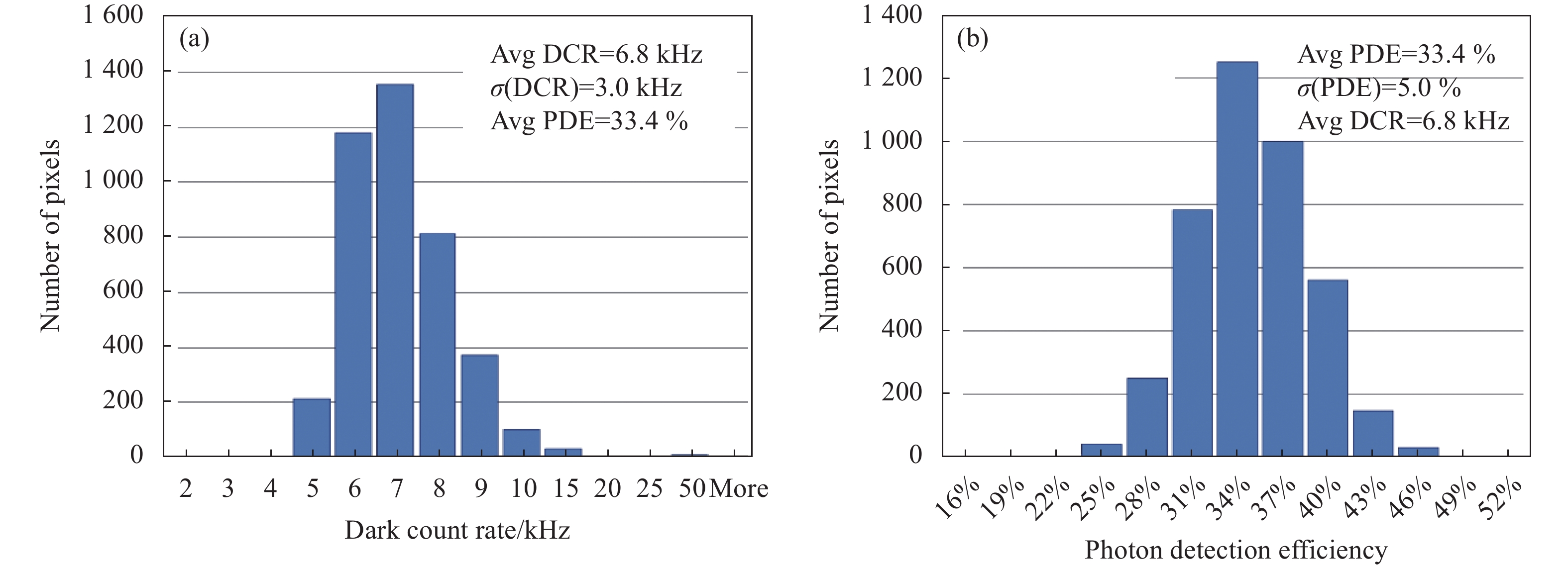
Chinese Academy of Sciences2022[7] 64×64 150 293 58.5±1.5 <1 - - Lincoln Laboratory 2018[26] 256×64 50 - 63±0.5 - 45% - 美国普林斯顿光波公司2014年[8]研制了具有单光子灵敏度的盖革模式焦平面阵列。该焦平面阵列包括三个部分:(1) InP/InGaAs 雪崩二极管阵列(PDA);(2) 定制硅CMOS 读出集成电路(ROIC);(3) 一个GaP微透镜(MLA)阵列,以提高有效填充因子。将InP/InGaAs PDA与定制硅ROIC耦合后,将MLA对准并集成到PDA背面实现了75%的有效填充因子。最后通过与陶瓷针插板的键合实现与ROIC的电气连接。其阵列包括32×32、128×32两种规格,其中32×32规格的焦平面阵列中像素间距为100 μm,而128×32规格的像素间距为50 μm。用1.06 μm的光照射两种规格的焦平面阵列,每个脉冲每个像素0.1光子,128×32规格的暗计数、探测效率测试结果统计如图12所示。在温度为253 K下,阵列的平均探测效率为33.4%,平均暗计数率为6.8 kHz。

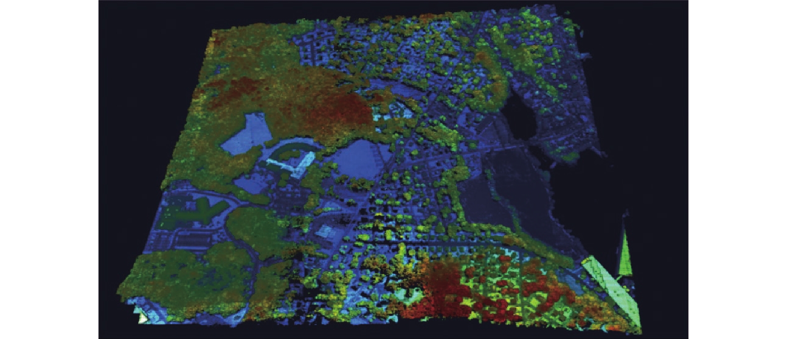
美国MIT林肯实验室(Massachusetts Institute of Technology,Lincoln Laboratory)报道了采用自研的256×64的1064 nm InP/InGaAsP SPAD焦平面阵列[27],阵列中心距50 μm,零度条件下探测效率25%,暗计数率10 kHz,完成了激光雷达三维成像,以下是对Maynard市500 m×500 m面积进行扫描的三维成像图,如图13所示,扫描时间10 s,其中的颜色含有距离信息。

日本滨松光子2018年[24]研制了规格为32×32,像素间距为100 μm的 InP/InGaAs SPAD焦平面阵列,通过在每个像素周围设置隔离槽,以防止相邻像素之间的光串扰,并阻断表面漏电流,采用倒装键合技术实现阵列与集成读出电路之间的互连。该阵列像素的击穿电压在60 V附近,在242 K时,阵列暗计数、探测效率统计图如图14所示,该阵列的平均暗计数率为234 kHz,99%的阵列像素暗计数率低于350 kHz。采用1550 nm的光源照射,阵列像素的探测效率为10%~12%。

国内重庆光电技术研究所、中国科学院半导体研究所也报道了研制的单光子焦平面探测器。2015年,重庆光电技术研究所[25]报道了规格为8×8,像元中心距为150 µm的InP/InGaAs 盖革模式焦平面阵列。该阵列采用ICP刻蚀形成隔离槽,阻断相邻单元载流子的耦合通路,抑制像元间的电串扰。在InP衬底背面采用光刻胶热熔法制作微透镜,实现微透镜阵列的单片集成。在背部其余区域蒸发金属层,作为n极共面引出,在各单元p型扩散区蒸发金属层形成p电极,通过In柱阵列制备与读出集成电路实现互连。该InP/InGaAs SPAD阵列的击穿电压为68 V±200 mV范围内呈正态紧密分布,标准偏差为80 mV;暗电流分布在0.2~0.4 nA范围内,其均值为0.273 nA,阵列均匀性较好。
2022年,中国科学院半导体研究所[7]设计了用于1550 nm波长的三维成像激光雷达系统的64×64 InP/InGaAs SPAD阵列,阵列中的二极管采用的是SAGCM结构,其有源区直径为25 μm,像素间距为150 μm。阵列击穿电压、暗电流统计如图15所示。阵列内大多数阵列像素的击穿电压在57 V和60 V之间,阵列击穿电压均匀地保持在±1.5 V的范围内,击穿电压处的暗电流低于1 nA。

2023年,中国科学院上海光学精密机械研究所联合中国电波传播研究所[28]共同研制了基于国内自研的InGaAs盖革模式雪崩光电二极管阵列探测器的小型化激光雷达系统样机。该样机可搭载于车载移动平台开展三维地形测绘,其结构组成主要包括以下五个模块:光纤激光器模块、阵列探测器模块、发射接收光学模块、扫描模块以及总控模块。其中探测器模块所用探测器为 64×64 InGaAs 盖革 APD 阵列,对于1550 nm波长的光量子效率为 20%,低温制冷条件下对应的暗计数率为20 kHz。该三维成像激光雷达系统成像性能良好,可实现动平台高分辨率三维成像。
-
通过在器件倍增层增加离化工程,采用噪声因子更小、带隙更宽且与吸收层InGaAs晶格匹配的In0.52Al0.48As作为倍增层、或采用数字合金新材料等方法以进一步提高短波红外单光子探测器的性能。
-
对于SAGCM结构的短波红外单光子探测器,载流子离化倍增时,存在死区效应而需要厚倍增层,这降低了器件的响应速度。因此,2006年,康塞普西翁大学[29]报告了具有能量积累层的分离吸收倍增层结构SPAD,该SPAD倍增层由宽带隙In0.52Al0.48As层(能量积累层)和InP层构成。由于能量积累层In0.52Al0.48As的离化能比InP的离化能高,InGaAs层中的光生空穴进入能量积累层后在电场的作用下积累能量,设计InAlAs层的宽度略小于空穴死区,空穴在InAlAs层中碰撞电离的概率为零,但空穴进入InP层时,其能量超过在InP中的电离阈值能量,因此,空穴进入InP倍增区将不需要空穴死区立即电离,这样既保证了器件的探测效率,同时降低了器件的过剩噪声因子。
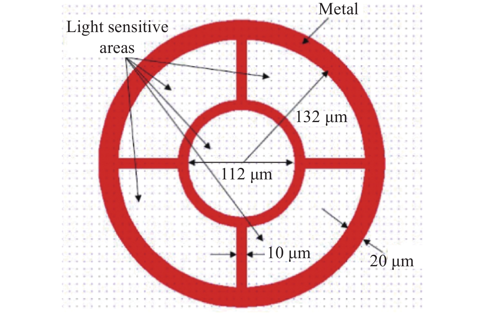
2018年,美国海军实验室报道了基于碰撞电离工程制成的InAlAs/InGaAs雪崩光电二极管阵列[30],该阵列的几何结构如图16所示,阵列包括一个中心像素和四个同心外围像素。阵列直径为为264 μm,中心元直径为112 μm,相邻元素之间的距离约为10 µm。阵列填充因子约为85%,对于1550 nm波长的光、超过80 GHz的增益带宽积下测得的器件量子效率约为84%。
-
倍增层材料除了空穴倍增的InP材料外,可以用与InGaAs晶格匹配、电子倍增的In0.52Al0.48As作为倍增材料。相比于InP,In0.52Al0.48As带隙更宽,雪崩击穿电压的温度依赖性相对InP更不敏感,因此InAlAs材料的SPAD工作温度具有灵活性。与 InP/InGaAs SPAD 相比, InGaAs/InAlAs SPAD 具有高增益带宽积、低过量噪声、低温度系数和高灵敏度等优点。
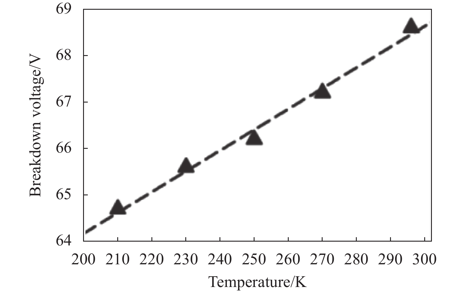
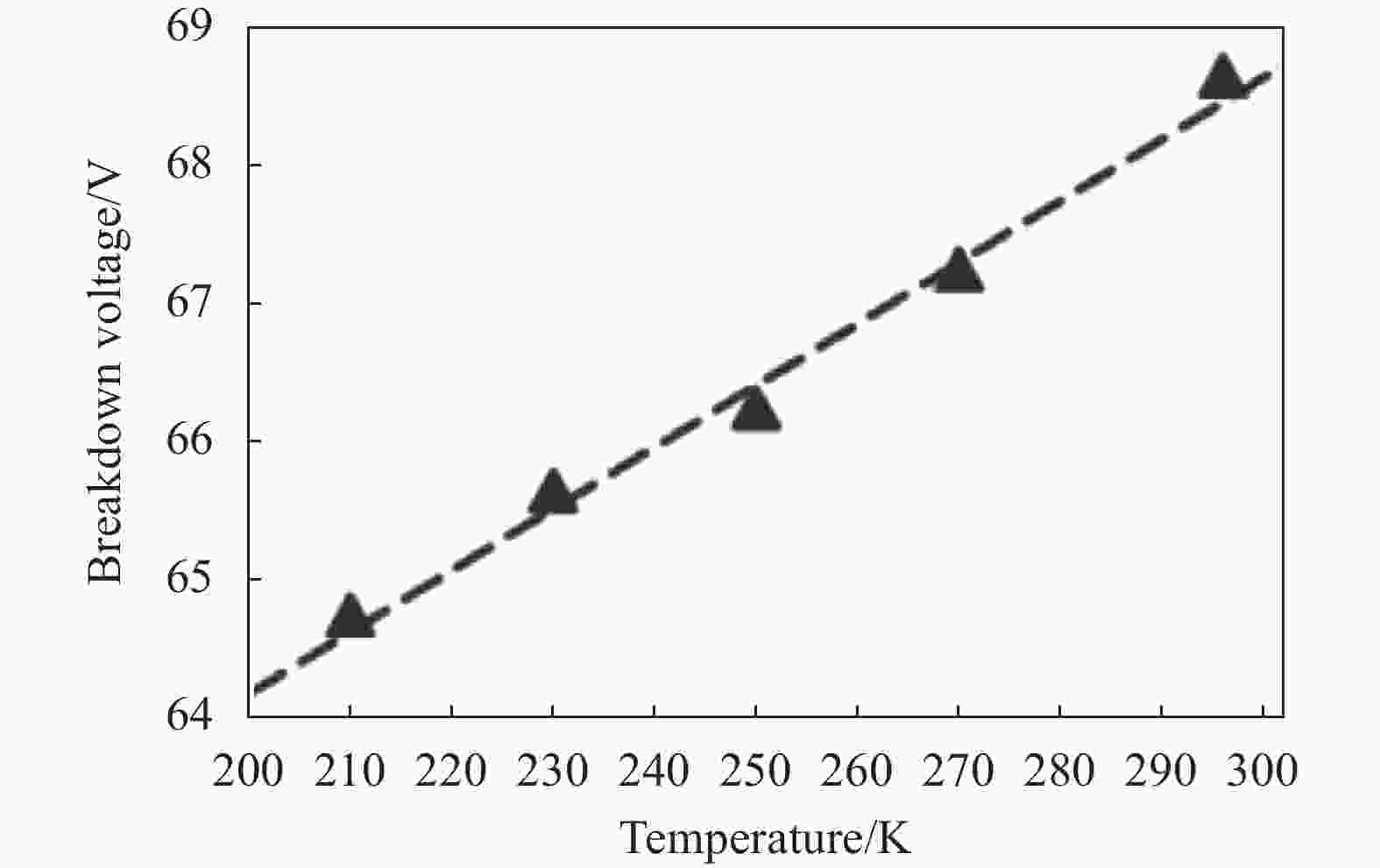
2016年,谢菲尔德大学[31]设计了用于探测1550 nm的InGaAs/InAlAs SPAD。该SPAD采用InP基底,1700 nm InGaAs作为吸收层,1000 nm InAlAs为倍增层。对该探测器进行了不同温度下击穿电压的测试,如图17所示。由图中可知InAlAs SPAD 的温度系数约为50 mV/K,小于InP材料的温度系数约100 mV/K。运行于门控模式下,对1550 nm的光,温度为210 K,探测效率为26%,暗计数率为108 Hz。
2021年,新加坡国立大学[32]设计制造了能够抑制表面漏电流和过早击穿的三台面InGaAs/InAlAs SPAD,结构如图18所示。该 InGaAs/InAlAs SPAD在150~270 K的范围内,测得击穿电压的温度系数为37.4 mV/K。在门控模式下,门控重复频率为15 kHz、脉冲宽度(半峰全宽)为20 ns、幅度为10 V的高斯脉冲,对于1550 nm的光,在240 K时探测效率为35%,暗计数率为3.3×10⁷ Hz。

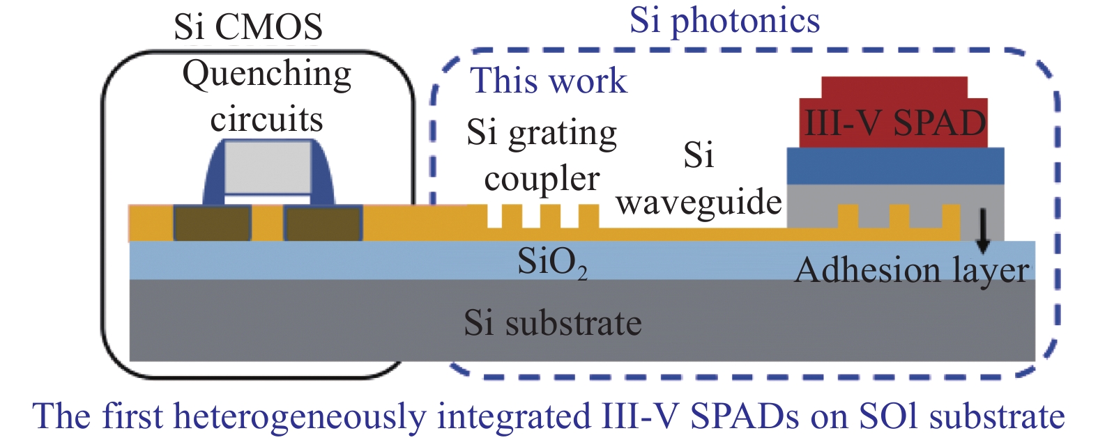
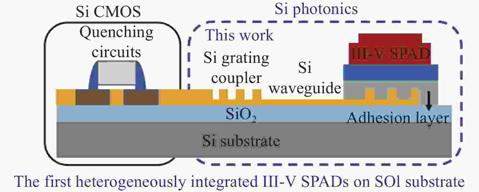
同年,新加坡国立大学[33]通过低温片间键合技术,首次在一个共同的SiO2平台上集成光栅耦合器、波导耦合器以及三台面InGaAs/InAlAs SPADs,如图19所示。对于1550 nm的光,在门控频率为15 kHz,门宽为20 ns的门控模式下,温度为220 K,获得探测效率约22%,暗计数率为8.6×10⁵ Hz。
2022年,华中科技大学[34]制造了平面 InGaAs/InAlAs SPAD ,器件截面图如图20所示,吸收层为1000 nm厚的未掺杂InGaAs,倍增层为200 nm厚的未掺杂InAlAs。对1550 nm的光,在门控频率为100 MHz的正弦门控模式下,温度为290 K,探测效率为10.4%,暗计数率为3.1 MHz。
-
GaSb基的AlxIn1−xAsySb1−y数字合金材料通过调整AlxIn1−xAsySb1−y中Al、Sb的成分可调整材料带隙,有望制成高性能的雪崩光电二极管。
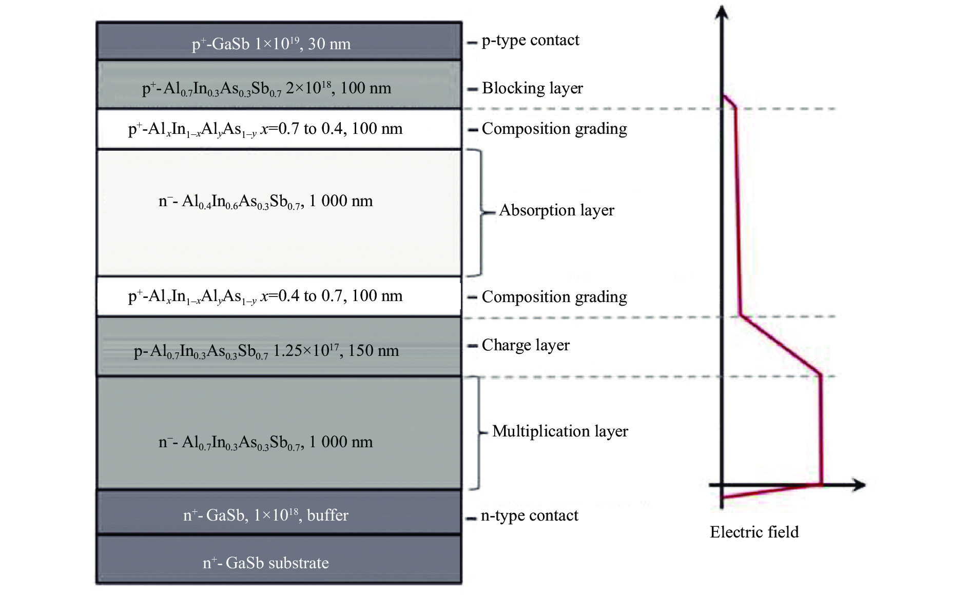
2018年,美国弗吉尼亚大学[35]制造了分离吸收、电荷、倍增(SACM)型的Al0.7In0.3As0.3Sb0.7/Al0.4In0.6As0.3Sb0.7雪崩光电二极管,结构图及内部电场分布图如图21所示。室温条件下器件处于95%击穿时,暗电流约为120 nA,与AlInAs/InGaAs APDs相当。将吸收层厚度调整为3 μm并在顶面上添加抗反射涂层,对于1550 nm的光实现了大于80%的量子效率。

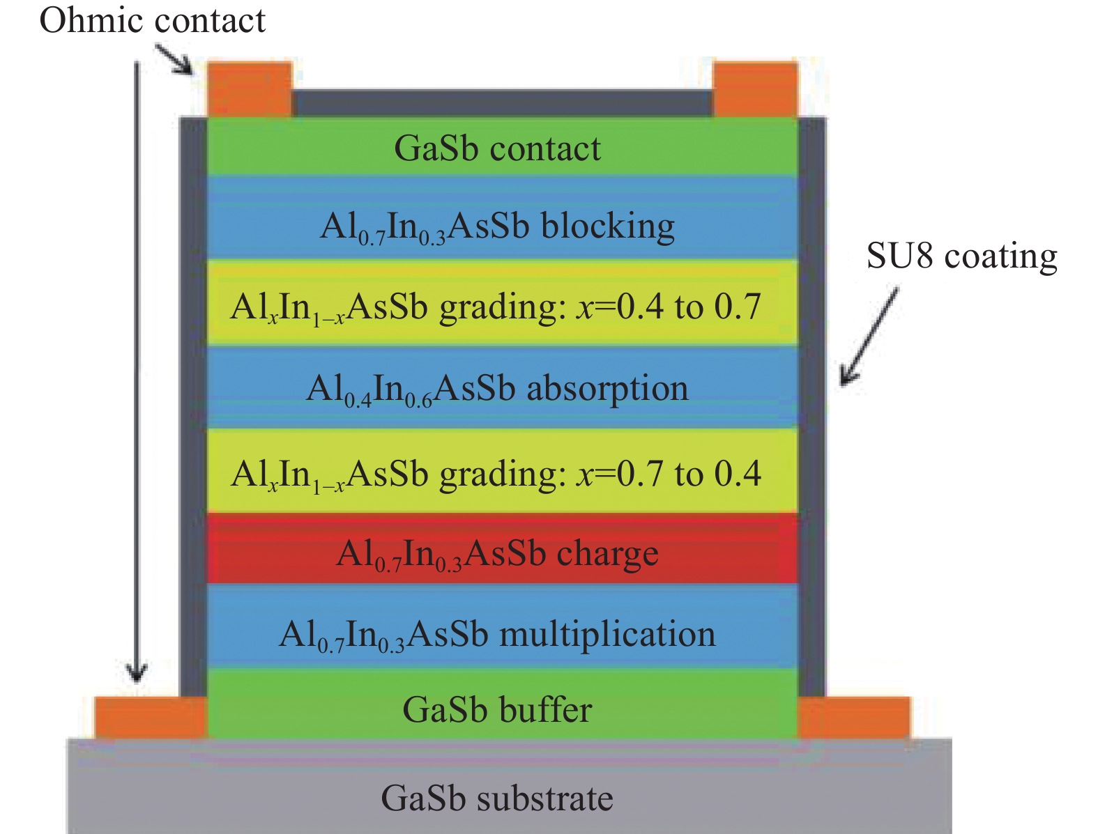
2020年,中国科学院半导体研究所[36]设计并制备了分离吸收、渐变、电荷和倍增(SAGCM)型的AlInAsSb数字合金雪崩光电二极管,结构图如图22所示。在室温下,该器件在击穿前获得的稳定增益高达100,95%击穿电压时暗电流密度为0.95 mA/cm2。

Sb基InAlAsSb合金材料制备的雪崩光电二极管具有与Si相当的低过剩量噪声因子,另外具有增益稳定、带隙可调、室温下暗电流密度低等优势,是发展高性能短波红外单光子探测器的一个重要材料选择。
-
近10年国内外研究团队通过优化器件结构、制备工艺以及雪崩信号提取电路显著提高了InP/InGaAs SPAD的性能,高探测效率、低暗计数率、室温InP/InGaAs 短波红外单光子探测器获得快速发展。提高工作温度到室温或零度以上高温,是降低后脉冲的一个有效解决途径,同时可显著减小封装体积、降低成本。具有更小温度系数、带隙更宽且与吸收层InGaAs晶格匹配的InGaAs/In0.52Al0.48As SPAD,其探测效率、暗计数率目前不如InP/InGaAs SPAD,需要进一步改进提高。随着对三维成像的巨大发展需求,单光子焦平面阵列在规格和性能方面的提升是目前单光子探测器研究的一个重要工作。InAl-AsSb合金材料制备的雪崩光电二极管显示了较高的量子效率和稳定的雪崩增益,有望应用于高性能短波红外单光子探测器制备。
Advancement of shortwave infrared single-photon detectors (invited)
-
摘要: InP/InGaAs短波红外单光子探测器(SPAD)是目前制备技术较为成熟且获得广泛应用的单光子探测器,通过半导体热电制冷(TEC)即可达到的工作温度(−40 ℃左右),具有体积小、成本低,方便安装和携带的应用优势;另外,基于常规半导体二极管的芯片制造工艺很容易实现大面阵单光子阵列,除了探测信号,还具备三维数字成像功能。国外包括美国、瑞士、意大利、韩国、日本等对InP/InGaAs SPAD进行了长期持续的研究,目前已研制出单管的货架产品,性能还在不断的优化和改进之中,其单光子探测器阵列呈现了清晰的三维成像效果,正在逐步应用。国内包括重庆光电技术研究所、中国科学院上海技术物理所、西南技术物理研究所、中国科学技术大学、云南大学等对InP/InGaAs SPAD芯片先后进行了器件设计和器件制备研究,目前单管的性能已经达到与国外报道相当的性能。国内单光子探测器阵列的研究获得了一定的进展,但芯片规模和器件性能有待提升。文中对国内外InP/InGaAs短波红外单光子探测器的发展,在设计和研制中存在的问题,以及近10年来的优化改进进行了介绍,重点介绍了高温、高速以及单光子焦平面阵列的发展,并结合新颖的离化工程和新的材料体系发展,分析了未来的短波红外单光子探测器的发展趋势。Abstract:
Signifacance InP/InGaAs shortwave infrared single-photon avalanche diodes (SPADs) have proved to be the most practical tool for the detection of near-infrared single-photon because of their small volume, near-room-temperature operation, and ease of integration and fabrication of a focal plane array based on the conventional semiconductor manufacturing process. They have achieved wide application including quantum secure communication, spectrum analysis, weak signal detection, Light Detection and Ranging (LiDAR), as well as self-driving vehicles considering the eye-safe laser requirement. etc. The further mass application depends on the performance and price of the SPADs, so the issues about the avalanche diode design and processing, as well as the solution are very important for accelerating the practical application. The review and analyses about the advancement of the shortwave infrared SPDs is very essential for both the academic research and application. Progress The separate absorption, grading, charge, and multiplication (SAGCM) structure has been used for InP/InGaAs SPADs since it was designed. This ensures the low electrical field in InGaAs absorption layer and high field in multiplication layer, then tunnelling current arising from high electrical field in absorption layer is remarkably suppressed, so the dark counts. Except for the essential material structure design, the electrical field uniformity in the multiplication layer also influences the performance such as the dark counts of the SPADs. The afterpulsing problem is another issue limiting the maximum count rate of the SPD in the current period. Focusing these issues of InP/InGaAs SPADs, solutions for them are concluded from the long-term study of InP/InGaAs SPADs.The high detection efficiency SPADs, room-temperature SPADs, and high count rate SPADs reported in the past decade by various institutions at home and abroad are summarized in detail. The typical performance parameter detection efficiency is improved by increasing the quantum efficiency via integrated absorption enhancement structure, the reported maximum value for 1 550 nm is 60%. The room temperature operation SPADs was carried out by both decreasing dark counts and sine-wave gated-quenching technology. About 20% detection efficiency and kHz dark counts at 293 K are acceptable for the practical application. Besides, the especial promising result for the room temperature SPDs is the reduced afterpulsing owing to the shortened carrier lifetime under the high temperature. The GHz SPDs benefit from the high and narrow sine-wave gate, as well as the simple harmonic wave noise out of the sine-wave gated-quenching technology. The typical performance parameter of high detection efficiency, room-temperature and high count rate InP/InGaAs SPDs are shown (Tab.1-Tab.3).Moreover, the InP/InGaAs SPAD focal plane arrays (FPAs) and the performance are concluded (Tab.4). The issues for the SPAD FPAs are mainly optical and electrical crosstalk between the adjacent pixels, solution such as mesa separation, microlens and optical filter, etc. are applied for decreasing the crosstalk. The clear three-dimensional image coded distance information was presented (Fig.13). The three-dimensional imaging with high sensitivity and long-distance detection ability attracts the enormous application requirement in both military and civil field. Finally, this paper introduces the novel SPDs technology including addition ionization engineering to the SPADs multiplication layer or using InAlAsSb digital alloys materials to further improve the performance. In0.52Al0.48As with smaller noise factor, wider band gap and matching the InGaAs lattice of the absorbing layer is used as the multiplication layer for electron ionization. Multiple layer ionization is applied to SPADs for increasing the ionization rate and detection efficiency. Conclusions and Prospects During the last decade the InP-based shortwave infrared single-photon detectors (SPDs) has gained the dramatic progress, the typical detection efficiency of the InP/InGaAs SPADs has been increased from 20% to 30%, and the dark count rate has been reduced to less than kHz. The high temperature SPADs up to room temperature operation, high speed SPADs up to GHz has appeared owing to the improvement of both avalanche diode and quench circuit. The single-photon focal plane arrays of 256×64 have also presented the clear three-dimensional image.The foreign countries including the United States, Switzerland, Italy, South Korea and Japan, etc. have performed long-term research on InP/InGaAs SPADs, and developed commercial self-products. Domestic research groups have successively prepared InP/InGaAs SPAD chips, and the performance is comparable to foreign reports. Furthermore, single-photon detector arrays have made certain progress, but the device format and performance need to be improved. Novel SPDs technology such as low noise factor material and ionization engineering are expected to further improve the performance. The high performance and low cost shortwave SPDs will further facilitate the quantity application including weak signal detection, LiDAR and digital imaging etc. -
图 1 (a) InP/InGaAs SPAD结构示意图;(b) 击穿时SPAD内部电场分布
Figure 1. (a) Schematic diagram of InP/InGaAs SPAD; (b) Electric field distribution inside SPAD at breakdown voltage
图 3 (a) 中国科学技术大学1.25 G正弦门控,不同温度、不同峰峰值条件下探测效率与暗计数的关系[6];(b) 中国科学技术大学金属层和三个周期的SiO2/TiO2布拉格反射镜组成的增强反射结构[1]
Figure 3. (a) Relationship between detection efficiency and dark counts rate under different temperatures and different peak-to-peak values with 1.25 G sinusoidal gating from University of Science and Technology of China[6]; (b) Enhanced reflection structure consisting of metal layer and three-cycle SiO2/TiO2 Bragg mirror made by University of Science and Technology of China[1]


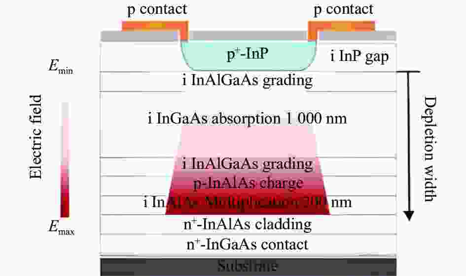
表 1 近10年报道的高探测效率InP/InGaAs SPAD的性能汇总
Table 1. Summary of the InP/InGaAs SPADs with high detection efficiency reported in the past decade
Institution Year Detection efficiency Temperature/K Dark count rate/kHz Time jitter/ps Afterpulse probability Politecnico di Milano 2012[3] >25% 225 100 <90 - 2014[4] 28% 225 few 87 - 2021[5] 11%-30% 225 1.46-6.47 340-119 1%-5.9% University of Science
and Technology of China2020[6] 40% 253 14.5 - 5.5% 2022[1] 30% 233 0.665 - About 15% Institute of Semiconductors,
Chinese Academy of Sciences2022[7] 25.72% 223 9.09 - - Princeton Lightwave 2014[8] 25% 225 6 - - 2020[9] >10% 233 <10 - <10% Chongqing Institute of
Optoelectronic Technology2017[10] 20% 223 1 - - Yunnan University 2022[11] 35.7% 233 3.3 - -  下载: 导出CSV
表 2 国内外报道的室温SPAD性能
Table 2. Performance of SPAD operating at room temperature
Institution Year Temperature/K Detection efficiency Dark count rate/kHz Afterpulse probability Time jitter/ps University of Shanghai for
Science and Technology2017[12] 293 21% 551 1.4% - Woorio Co Ltd 2021[13] 293 20.9% 5.1 0.8% - École Polytechnique
Fédérale de Lausanne2022[14] 300 43% 4000 - 109 National University of
Defense Technology2018[15] 294 10.6% 2.5×10⁻⁵/gate 1.3% -
下载: 导出CSV
表 3 近10年报道的高计数率InP/InGaAs SPAD的性能汇总
Table 3. Summary of the InP/InGaAs SPADs with high count rate reported in the past decade
Institution Year Method Frequency/
GHzTemperature/
KDetection
efficiencyDark count rate/
kHzAfterpulse
probabilityNihon University 2020[16] Sine-wave gating 1.27 289 55.9% 2350 4.8% Toshiba Research Europe Ltd 2015[17] Self-
differencing1 293 55% - 10.2% University of Science and
Technology of China2020[6] Sine-wave gating 1.25 300 60.1% 744 14.8% ID Quantique 2019[18] Dual anode SPAD 1 253 20.4% 54.25 3.5%
下载: 导出CSV
表 4 近10年SPAD焦平面阵列性能汇总
Table 4. Summary of SPAD focal plane array performance in the past ten years
Institution Year Format/
pixelPixels pitch/
µmTemperature/
KBreakdown voltage/
VDark current/
nAAverage detection
efficiencyAverage dark count
rate/kHzPrinceton Lightwave 2014[8] 32×32
128×32100
50248
353-
--
-30.5%
33.4%2.2
6.8Hamamatsu Photonics 2018[24] 32×32 100 242 60 - - 234 Chongqing Optoelectronics
Research Institute2015[25] 8×8 150 235 68±0.2 0.273 19.5% 32.5 Institute of Semiconductors,
Chinese Academy of Sciences2022[7] 64×64 150 293 58.5±1.5 <1 - - Lincoln Laboratory 2018[26] 256×64 50 - 63±0.5 - 45% -
下载: 导出CSV
-
[1] Zhang B, Yin S, Liu Y, et al. High performance InGaAs/InP single-photon avalanche diode using DBR-Metal reflector and backside micro-lens [J]. Journal of Lightwave Technology, 2022, 40(12): 3832-3838. doi: 10.1109/JLT.2022.3153455 [2] Liu J, Xu Y, Li Y, et al. Ultra-low dead time free-running InGaAsP single-photon detector with active quenching [J]. Journal of Modern Optics, 2020, 67(13): 1184-1189. doi: 10.1080/09500340.2020.1817591 [3] Tosi A, Acerbi F, Anti M, et al. InGaAs/InP single-photon avalanche diode with reduced afterpulsing and sharp timing response with 30 ps tail [J]. IEEE Journal of Quantum Electronics, 2012, 48(9): 1227-1232. doi: 10.1109/JQE.2012.2208097 [4] Tosi A, Calandri N, Sanzaro M, et al. Low-noise, low-jitter, high detection efficiency InGaAs/InP single-photon avalanche diode [J]. IEEE Journal of Selected Topics in Quantum Electronics, 2014, 20(6): 192-197. doi: 10.1109/JSTQE.2014.2328440 [5] Signorelli F, Telesca F, Conca E, et al. Low-noise InGaAs/InP single-photon avalanche diodes for fiber-based and free-space applications [J]. IEEE Journal of Selected Topics in Quantum Electronics, 2021, 28(2): 1-10. doi: 10.1109/JSTQE.2021.3104962 [6] Fang Y, Chen W, Ao T, et al. InGaAs/InP single-photon detectors with 60% detection efficiency at 1550 nm [J]. Review of Scientific Instruments, 2020, 91(8): 83102. doi: 10.1063/5.0014123 [7] Wang S, Ye H, Geng L, et al. Design, fabrication, and characteristic analysis of 64×64 InGaAs/InP single-photon avalanche diode array [J]. Journal of Electronic Materials, 2022, 51(5): 2692-2697. doi: 10.1007/s11664-022-09531-9 [8] Itzler M A, Entwistle M, Krishnamachari U, et al. SWIR Geiger-mode APD detectors and cameras for 3D imaging[C]//Pro-ceedings of SPIE, 2014, 9114: 91140F. [9] Beijing RMY Electronics Ltd. Pigtailed Coaxial Single Photon Avalanche Diode (SPAD) PGA-314-501. Product Descrip-tion[Z], 2020. [10] Li Bin, Chen Wei, Huang Xiaofeng, et al. InP cap layer doping density in InGaAs/InP single-photon avalanche diode [J]. Journal of Infrared and Millimeter Waves, 2017, 36(4): 420-424. (in Chinese) doi: 10.11972/j.issn.1001-9014.2017.04.007 [11] Liu C, Ye H, Shi Y. Advances in near-infrared avalanche diode single-photon detectors [J]. Chip, 2022, 1(1): 100005. doi: 10.1016/j.chip.2022.100005 [12] Liang Y, Chen Y, Huang Z, et al. Room-temperature single-photon detection with 1.5-GHz gated InGaAs/InP avalanche photodiode [J]. IEEE Photonics Technology Letters, 2017, 29(1): 142-145. doi: 10.1109/LPT.2016.2630273 [13] Baek S, Yang S, Park C, et al. Room temperature quantum key distribution characteristics of low-noise InGaAs/InP single-photon avalanche diode [J]. Journal of the Korean Physical Society, 2021, 78(7): 634-641. doi: 10.1007/s40042-021-00111-4 [14] Kizilkan E, Karaca U, Pesic V, et al. Guard-ring-free InGaAs/InP single-photon avalanche diode based on a novel one-step Zn-diffusion technique [J]. IEEE Journal of Selected Topics in Quantum Electronics, 2022, 28(5): 1-9. doi: 10.1109/JSTQE.2022.3162527 [15] Chen H, Jiang M, Sun S, et al. Room temperature continuous frequency tuning InGaAs/InP single-photon detector [J]. AIP Advances, 2018, 8(7): 75106. doi: 10.1063/1.5030141 [16] Tada A, Namekata N, Inoue S. Saturated detection efficiency of single-photon detector based on an InGaAs/InP single-photon avalanche diode gated with a large-amplitude sinusoidal voltage [J]. Japanese Journal of Applied Physics, 2020, 59(7): 72004. doi: 10.35848/1347-4065/ab9625 [17] Comandar L C, Fröhlich B, Dynes J F, et al. Gigahertz-gated InGaAs/InP single-photon detector with detection efficiency exceeding 55% at 1550 nm [J]. Journal of Applied Physics, 2015, 117(8): 83109. doi: 10.1063/1.4913527 [18] Park C, Cho S, Park C, et al. Dual anode single-photon avalanche diode for high-speed and low-noise Geiger-mode operation [J]. Optics Express, 2019, 27(13): 18201. doi: 10.1364/OE.27.018201 [19] Namekata N, Sasamori S, Inoue S. 800 MHz single-photon detection at 1550-nm using an InGaAs/InP avalanche photo-diode operated with a sine wave gating [J]. Opt Express, 2006, 14(21): 10043-10049. doi: 10.1364/OE.14.010043 [20] Namekata N, Adachi S, Inoue S. High-Speed Single-photon Detection Using 2-GHz Sinusoidally Gated InGaAs/InP Avalanche Photodiode[M]. Berlin, Heidelberg: Springer, 2009: 34-38. [21] Namekata N, Takesue H, Honjo T, et al. High-rate quantum key distribution over 100 km using ultra-low-noise, 2-GHz sinusoidally gated InGaAs/InP avalanche photodiodes [J]. Opt Express, 2011, 19(11): 10632-10639. doi: 10.1364/OE.19.010632 [22] Jun Zhang, Patrick Eraerds, Nino Walenta, et al. 2.23 GHz gating InGaAs/InP single-photon avalanche diode for quantum key distribution[EB/OL]. (2010-02-17)[2022-12-30]. https://arxiv.org/abs/1002.3240. [23] Yuan Z L, Kardynal B E, Sharpe A W, et al. High speed single photon detection in the near infrared [J]. Applied Physics Letters, 2007, 91(4): 41114. doi: 10.1063/1.2760135 [24] Baba T, Suzuki Y, Makino K, et al. Development of an InGaAs SPAD 2D array for flash LIDAR[C]//Proeedings of SPIE, 2018,10540: 105400L. [25] Zhang Xiuchuan, Jiang Liqun, Gao Xinjiang, et al. Fabrication of InGaAs/InP Geiger-mode avalanche focal plane arrays [J]. Semiconductor Optoelectronics, 2015, 36(3): 356-360. (in Chinese) [26] Aull B F, Duerr E K, Frechette J P, et al. Large-format Geiger-mode avalanche photodiode arrays and readout circuits [J]. IEEE Journal of Selected Topics in Quantum Electronics, 2018, 24(2): 1-10. doi: 10.1109/JSTQE.2017.2736440 [27] Albota M A, Gurjar R, Mangognia A, et al. The airborne optical systems testbed (AOSTB)[Z]. Lexington, Massachusetts, United States: MIT Lincoln Laboratory, 2017. [28] Chen Yongqiang, He Yan, Luo Yuan, et al. Pulsed three-dimensional imaging lidar system based on Geiger-mode APD array [J]. Chinese Journal of Lasers, 2023, 50(2): 0210001. (in Chinese) [29] Ramirez D A, Hayat M M, Karve G, et al. Detection efficiencies and generalized breakdown probabilities for nanosecond-gated near infrared single-photon avalanche photodiodes [J]. IEEE Journal of Quantum Electronics, 2006, 42(2): 137-145. doi: 10.1109/JQE.2005.861627 [30] Ferraro M S, Rabinovich W S, Mahon R, et al. Position sensing and high bandwidth data communication using impact ionization engineered APD arrays [J]. IEEE Photonics Technology Letters, 2019, 31(1): 58-61. doi: 10.1109/LPT.2018.2882886 [31] Meng X, Xie S, Zhou X, et al. InGaAs/InAlAs single photon avalanche diode for 1550 nm photons [J]. Royal Society Open Science, 2016, 3(3): 150584. doi: 10.1098/rsos.150584 [32] Zhang J, Wang H, Zhang G, et al. High-performance InGaAs/InAlAs single-photon avalanche diode with a triple-mesa structure for near-infrared photon detection [J]. Optics Letters, 2021, 46(11): 2670-2673. doi: 10.1364/OL.424606 [33] Zhang Jishen, Xu Haiwen, Zhang Gong, et al. First InGaAs/InAlAs single-photon avalanche diodes (SPADs) heterogeneously integrated with Si photonics on SOI platform for 1550 nm detection[C]//2021 Symposium on VLSI Circuits, 2021. [34] Tian Y, Li Q, Ding W, et al. High speed and high sensitivity InGaAs/InAlAs single photon avalanche diodes for photon counting communication [J]. Journal of Lightwave Technology, 2022, 40(15): 5245-5253. doi: 10.1109/JLT.2022.3174962 [35] Bank S R, Campbell J C, Maddox S J, et al. Avalanche photodiodes based on the AlInAsSb materials system [J]. IEEE Journal of Selected Topics in Quantum Electronics, 2018, 24(2): 1-7. doi: 10.1109/JSTQE.2017.2737880 [36] Zheng Danong, Su Xiangbin, Xu Yingqiang, et al. High gain and low dark current AlInAsSb avalanche photodiodes grown by quaternary digital alloys [J]. Journal of Infrared and Millimeter Waves, 2021, 40(2): 172-177. (in Chinese) doi: 10.11972/j.issn.1001-9014.2021.02.006 -

 点击查看大图
计量
- 文章访问数: 426
- HTML全文浏览量: 36
- PDF下载量: 251
- 被引次数: 0

