


-
无线光通信(OWC)是依靠光辐射来传递信息,光的波长可以从红外(IR)到深紫外线(UV)[1]。而与长波长光通信相比,深紫外光通信具有许多优点。首先,大部分的太阳紫外线辐射,特别是200~280 nm之间的UV-C波段,会被地球平流层的臭氧层吸收,能抵达地面的深紫外(DUV)线辐射非常少[1]。因此,在室内外进行的深紫外光无线通信的背景噪声可以忽略不计[2],紫外光通信的信噪比远高于长波长光通信;第二,由于紫外光在空气中的散射较强,紫外光通信无需具备一系列对准、跟踪和捕获等复杂路线设计,其能够以散射的方式直接实现非直视(NLOS)通信。此外,深紫外光的辐射功率随传输距离呈指数衰减,限制了信号传播,信号难以被远距离监听和截获[3]。而如果在卫星之间通信采用深紫外光通信技术,那么第三方在地面上也无法监测到光信号,使深紫外光通信具备非常高的光通信安全性。由上述优点可知,深紫外光通信在光通信,尤其是保密通信方面的发展潜力非常大。
AlGaN基μLED的发射波长可从210 nm调节到360 nm,覆盖了整个日盲光谱,且具有高调制速度和低功耗的优点,是最理想的深紫外通信光源。但是当前深紫外LED低的发光效率严重限制了其在日盲光通信中的应用。如图1所示,是一个以蓝宝石基板作为衬底,由n型和p型AlGaN层包围的AlGaN多量子阱的典型深紫外LED结构。在p型侧的上方是p-GaN层提供空穴注入并作为欧姆接触层。当前深紫外LED的效率受到许多因素的制约,一方面,蓝宝石通常被用作紫外LED的衬底,由于蓝宝石与空气折射率差别较大会造成严重的内部全反射,衬底侧的光提取效率(LEE)会受到限制[4-5]。而高铝组分的AlGaN发出的光中横向传播的TM极性的光占比非常大,这进一步加剧了全内反射限制光的比例。同时蓝宝石衬底和AlGaN之间较大的晶格不匹配,导致了AlGaN层较高的穿透位错密度(TDD),进一步影响LED的性能。另一方面,高Al组分AlGaN材料难以获得较高的n型与p型掺杂效率,欧姆接触不易制备从而导致高工作电压和低电光转换效率[6]。通常在p-AlGaN层的顶部生长p-GaN层,以提供更好的欧姆接触和改进的空穴供应。但p-GaN层对紫外光的强吸收导致光提取效率较低[7],这也是深紫外发光器件经常采用倒装结构的重要原因之一。许多技术被用来改善深紫外LED的晶体质量和发光效率。一些先进的技术可以抑制蓝宝石衬底上生长的高Al组分AlGaN层中的TDD,如迁移增强金属有机化学气相沉积[8],缓冲层技术[9-10]与蓝宝石图形衬底技术[11]。此外,通过使用不具有p-GaN接触层的UV透明p-AlGaN异质结构以及具有高反射的p接触电极,可以降低p型层吸收从而提高DUV LED效率[12-13]。另外,LED的台面通常是通过干法刻蚀制备,这会在侧壁引入非常多的侧壁缺陷。而当LED尺寸减少时,电流的扩展效应会增强,从而使载流子更容易到达台面边缘的侧壁缺陷区域,导致显著的表面非辐射复合,从而降低了效率[14-15]。而低的发光效率,带来了自热效应严重,在注入大电流下存在严重的由于热而引起的功率下降。这将导致器件无法工作在注入的大电流下,从而无法实现单芯片高功率的输出。

图 1 DUV LED器件典型的外延结构图
Figure 1. Typical epitaxial structure diagram of DUV LED devices
文中系统回顾了深紫外LED在日盲光通信里面的应用和当今发展的现状,详细介绍了尺寸效应对深紫外μLED在光电热等方面的影响及物理机制,并对提高μLED的光提取效率与散热的几种方法进行详细的阐述。
-
实现深紫外光通信的一个关键器件是深紫外光源。早期深紫外光源利用高压汞灯实现,但汞灯的调制带宽非常小,这严重影响了深紫光通信的传输速率。最近几年,随着深紫外LED技术的不断发展[16-19],深紫外LED的高调制带宽、低功耗及设计灵活的特性使其在深紫外光通信领域受到越来越多的关注。尤其是随着高效率商用化的深紫外LED的出现,并且实现寿命大于1000 h。采用深紫外LED作为日盲紫外光通信的光源技术已经开始具备实际应用价值并快速成为当前研究热点。2002年,SET (Sensor Electronic Technology) 公司生产出了可以商用化的波长在247~365 nm之间的深紫外LED,而美国麻省理工大学林肯实验室首先在2004年进行了利用深紫外LED尝试完成紫外光通信的设计[20]。根据香农定理,通信中的数据传输速率由带宽和信噪比决定。为了增加传输速率,必须尽量增加光源带宽和提高信噪比。而光源的调制带宽直接受RC时间常数的制约[21-23],对器件电容(C)有很强的依赖性。C随着器件尺寸的减小而减小[24-25],因此实现快速调制的关键技术是缩小LED器件尺寸,特别是小于100 μm×100 μm,即微型发光二极管(μLED)。
目前,基于DUV μLED下进行的无线光通信的研究中,紫外通信的带宽和数据传输速率已经达到了前所未有的水平。2019年,He等将直径小于100 μm的深紫外μLED应用到深紫外通信系统里面,其用尺寸为566 μm2的芯片,系统带宽在71 A/cm2条件下达到438 MHZ[26]。Zhu等[27]阐述在基于276.8 nm的短波紫外线μLED的紫外通信系统中,电流密度为400 A/cm2的条件下,获得452.53 MHz的−3 dB带宽和0.854 mW的光输出功率。采用16位正交调幅正交频分复用和预均衡技术,实现长度在0.5 m以上,数据速率为2 Gb/s的紫外通信链路。此外,Maclure等[28]采用了一个由8个梯形像素组成的深紫外μLED阵列,每个像素的面积相当于直径约40 µm的圆形器件,调制带宽最大可达915 MHZ,并实现了在10 m处大于6 Gb/s和在17 m处大于4 Gb/s的数据速率,其进一步采用紫外μLED,且通过优化系统参数来提高光通信系统的性能[29],分别在10 m和60 m处实现6.5 Gb/s和4 Gb/s的数据速率,其调制带宽最大可达960 MHz。表1总结了DUV LED作为光源时,光通信中带宽和数据传输速率的发展情况。
表 1 LED作为光源时紫外通信的发展
Table 1. Development of UV communication with LED as a light source
Year Bandwidth/MHz Modulation scheme Distance/m Data rate Ref. 2022
2022
2021960
915
452OFDM
OFDM
OFDM10
17
0.56.50 Gb/s
>4 Gb/s
2 Gb/s[29]
[28]
[27]2020 170 PAM-16 1 2.4 Gb/s [30] 2020 170 PAM-16 5 1.09 Gb/s [31] 2019 438 OFDM 0.3 1.1 Gb/s [26] 2019 153 - 1.5 1.18 Gb/s [32] 2018 153 PAM-4 1.6 1.6 Gb/s [2] 2018 1.9 - 150 921.6 Kb/s [33] 2018 20 OOK - 1.92 Mb/s [34] 2017 29 OFDM - 71 Mb/s [35] 从通信系统的带宽和数据传输速率可以看出,DUV μLED的运用提高了带宽。同时,在同一调制方式下,带宽越大,能达到的最大数据传输速率就越高。此外,由于紫外光功率在大气中的快速衰减,当数据传输范围较远时,传输速率会下降。因此保证大的调制带宽的同时提高深紫外μLED的光输出功率,是DUV μLED光通信系统获得高速传播的关键。当深紫外LED尺寸变小时,会使调制带宽变大,但是其有源区面积的减少也导致相同电流密度下光功率急剧下降。而深紫外光在空气中传播很容易被吸收,这严重影响了特定距离的光信号信噪比。而为了解决这一矛盾点,可以通过对单颗芯片加大电流实现。但是深紫外LED较低的发光效率和严重的侧壁缺陷辅助的非辐射复合,导致大电流下存在严重的自发热效应,功率无法随着电流持续增加。因此,要实现高传播速度的深紫外μLED光通信,关键点是使深紫外μLED具有高调制带宽、发光效率好、散热能力好等特性。
-
首先,尺寸会严重影响μLED的调制带宽。由于μLED比大尺寸LED的尺寸减少,且整体表面积比增加,因此μLED具有较低的电容、较好的散热效应和良好的电流扩展,所以μLED工作电流密度可以比大尺寸LED更高。表征LED调制带宽的−3 dB响应频率f−3 dB的关系式可表示为[36]:
$$ {f}_{-3\;{\rm{dB}}}=\frac{\sqrt{3}}{2\pi \tau }=\frac{\sqrt{3}}{2\pi }\left(\frac{1}{{\tau }_{r}}+\frac{1}{{\tau }_{nr}}+\frac{1}{{\tau }_{RC}}\right) $$ (1) 式中:τ为少数载流子的寿命;τr为辐射载流子的寿命;τnr为非辐射载流子的寿命;τRC为RC时间常数。对于尺寸为100 μm×100 μm及以下的LED,载流子辐射寿命是限制调制带宽的主要因素。在这种情况下,载流子辐射寿命取决于注入的电流密度,τr= 1/B×N,其中B和N分别表示辐射系数和载流子密度。因此,假设存在双分子重组机制时,f−3 dB符合如下公式[37]:
$$ {f}_{-3\;{\rm{dB}}}=\frac{\sqrt{3}}{2\pi }\times \left(\sqrt{\frac{BJ}{qd}}+\frac{1}{{\tau }_{nr}}+\frac{1}{{\tau }_{RC}}\right) $$ (2) 式中:J为注入电流密度;q为基本电荷;d为有源区厚度。因此,公式(2)表明,通过增加工作电流密度或减小芯片尺寸,可以实现更高的−3 dB带宽。
随着μLED尺寸减小,其芯片电容随之减小,同时其可工作在较高的电流密度下,从而缩短内部差分载流子寿命,因而小尺寸μLED获得更高的调制带宽[38]。Maclure等[39]对DUV μLED的尺寸依赖研究表明,器件的带宽有明显的尺寸依赖性,器件越小,带宽越高,20 μm器件的带宽达到570 MHz。Qian等[40]研究了基于整个通信系统的UVC LED的尺寸效应。他们发现随着电流的增大,μLED的−3 dB带宽不断增大。此外,小尺寸LED具有更高的调制带宽,并且随着电流密度的增加,LED调制带宽迅速增加。然后,随着电流的进一步增加,调制带宽趋于饱和甚至略有下降。带宽下降可能是热效应造成的,如载流子溢出,导致辐射复合效率下降,有效载流子寿命增加,从而降低调制带宽[28]。另外,提高深紫外LED的带宽还可以利用等离子激元[41-42]与微腔[43]等技术。Zhang等[42]通过将高密度的Al纳米三角阵列转移到μLED的指定p-AlGaN区域,实现了局域表面等离子体共振耦合的效果,以提高−3 dB的调制带宽。但由于μLED较小的有源区面积,等离子激元与微腔技术在小尺寸深紫外LED中应用很少,还需科研工作者的努力探索。
其次,μLED尺寸严重影响芯片的I-V特性曲线。随着芯片整体直径(D)减小从而导致串联电阻增加,串联电阻近似与D−2成正比[44]。即台面尺寸越小,串联电阻越大,即相同工作电流下,小尺寸的芯片工作电压急剧升高,如图2(a)所示。但是如果考虑电流密度的话,在相同工作电压下,小尺寸的器件电流密度更大,如图2(b)所示,这是由于器件整体面积减小的原因。另外 ,还需要注意到,随着器件尺寸减少,其电流扩展效应是更好的,这能使电流分布更均匀,从而使器件可以承受更大的电流密度,这将非常有利于提高调制带宽特性。

图 2 (a) I–V特性曲线的尺寸依赖性;(b)相同电压下电流密度的尺寸依赖性[44] ;(c) 有侧壁损伤的LED A、B、C的示意结构(LED A、B和C的可用面积比分别为85%、75%和36%[45])
Figure 2. (a) Size-dependent I–V characteristics curves; (b) Size dependence of current density under the same voltage[44]; (c) LEDs A, B, C with sidewall damages (The usable area ratios for LEDs A, B and C are 85%, 75% and 36%[45])
除此之外,LED器件的漏电流也表现出尺寸依赖性。由于较高的表面积体积比,台面尺寸较小的LED的漏电流往往较大,因为台面边缘的侧壁缺陷会作为漏电流通道[44]。随着芯片尺寸的减少,由于刻蚀台面而引起的侧壁缺陷所占有的整个芯片的面积将急剧增加,如图2(c)所示。因此,与大尺寸LED器件不同,由侧壁缺陷引起的表面非辐射复合是µLED的不可忽略的影响因素[45]。
第三,随着μLED的芯片尺寸减小,其光提取效率能得到有效提升。这是由于更小的芯片尺寸能使光更快逃离,从而减少被芯片内部吸收材料的吸收概率。Floyd等通过阴极发光线扫描实验测量器件的深紫外发射的横向吸收长度[46]。将阴极发光线扫描强度映射到扫描电子显微镜(SEM)测量的台面直径,可得到台面结构内的横向吸收长度约为15 μm。在尺寸越小的LED中,光子横向传输距离越短,从而光子抵达侧壁并逃逸之前被吸收的比例越小,从而改善了器件的LEE。另外,通过FDTD模拟也表明,对于有倾斜侧壁的深紫外LED,其尺寸越小,光提取效率越高,如图3所示。具有倾斜侧壁结构的LED尺寸的减小使更多横向传输的光子首先抵达到倾斜侧壁而不是AlGaN与蓝宝石的界面,从而使更多的光子尽快被倾斜侧壁反射到逃离锥里面,有效提高了光提取效率。

图 3 FDTD中模拟的TM偏振光的光提取效率与尺寸的关系
Figure 3. Relationship between light extraction efficiency and size of TM polarized light simulated in FDTD
第四,芯片尺寸对于光功率有非常重要的影响。如图4(a)所示,随着芯片尺寸面积的减小,在相同工作电流下,小尺寸器件整体的光功率比大尺寸器件要小。从前面分析可知,尽管尺寸减小,其光提取效率得到提升,但是由于小尺寸芯片好的电流扩展和高的侧壁缺陷面积比,导致侧壁缺陷引起的非辐射复合增加更大,从而使整体的光功率下降。但由于小尺寸器件面积更小,电流扩展效应更好的原因,它能承受更高的电流密度,有较高的光功率密度,如图4(b)所示。值得注意的是,最小的器件(D=20 μm)的最大功率密度可达86 W/cm2,比最大的器件(D=300 μm)的最大功率密度(4.14 W/cm2)高出20倍以上。图2(b)可以佐证较小台面尺寸的LED可以承受更高的电流密度,最小的LED可以承受的正向电流密度达到4500 A/cm2以上。而光提取效率的增加也会促使小尺寸的LED具有更高的光功率密度。2022年,中国科学院半导体研究所Guo等[47]研究了并联的深紫外μLED阵列结构的尺寸效应,其也发现了类似的现象。随着尺寸减少,在相同电流密度下,由于小尺寸μLED面积小,总电流更小并且非辐射复合更严重,导致小尺寸μLED阵列的光功率更小。但是小尺寸μLED的光功率密度是更大的,这是因为减小芯片尺寸可以减少光子抵达高吸收的电极,从而减少光逃离路径的损耗,增加了光提取效率,获得更高的光功率密度。
另外,从图4(a)和(b)可以看到,随着芯片尺寸减少,器件功率饱和电流减少,但是功率饱和电流密度却是增加的。功率饱和电流的减少,主要是由于芯片尺寸减少,串联电阻增加,在相同电流下其发热量增加。而功率饱和电流密度增加一方面是由于体表面积随着芯片尺寸增加,从而小尺寸芯片表面散热能力更强;另一方面是由于小尺寸芯片具有更好的光提取效率,导致更多光被提取,而不是被吸收转化成热,从而进一步减少了热的产生。因此可以看到,μLED尽管可以承受大的电流密度,但是却无法承受和常规LED一样大的电流,主要是由于严重的热效应使得器件的功率过早趋于饱和甚至下降[48-50],这限制了μLED利用大电流去进一步的提升光功率。而严重的热效应也会导致μLED发射波长红移和器件寿命减少[51]。

图 4 (a)不同台面尺寸的DUV LED的光输出功率作为注入电流的函数;(b)光功率密度的尺寸依赖性[44] ;(c)三种研究器件在不同电流下的光输出功率和DUV LED的LEE增强因子(d)[52]
Figure 4. (a) Light output power as a function of injection current for the DUV LEDs with different mesa sizes; (b) Size dependence of optical power density[44] ; (c) Light output power and (d) the LEE enhancement factor of the DUV LEDs at different currents for the three investigated devices[52]
综上所述,器件尺寸变小时可以有效改善电流拥挤增加带宽,提高器件的光提取效率,提升器件工作的最大电流密度和功率密度,但有源区面积的减小使得侧壁非辐射复合增加,串联电阻变大,自热效应严重,输出功率减小。当设计出合适的阵列形式的μLED时,相比较单个μLED的情况下可以弥补较低的输出光功率[52]。中国科学院半导体研究所利用4×4的阵列使光输出功率达到mW级,并实现了380 MHz的调制带宽[47]。而Yu等[53]设计并制造了一个由10×10个μLED组成的深紫外发光阵列,并对发光阵列的电学和光学行为进行了系统的研究。与具有相同发射面积的传统大型LED芯片相比,该阵列在100 mA的注入电流下,总光输出功率显著提高,DUV μLEDs阵列中单个LED尺寸变小时电流扩展效应更好,因此功率明显表现出随LED尺寸变小而变大的特性,如图4(c)所示。此外,图4(d)显示了通过μLED阵列与平面LED的EQE之比获得的LEE增强因子。μLED阵列(50 μm)和μLED (20 μm)的LEE分别是平面LED的1.3倍和1.5倍。这是由于尺寸的减小,使侧壁处的光反射增强以及光子的横向传播距离缩短。此外,μLED阵列的LEE增强因子在较高的注入电流水平下更大。这些结果表明,μLED阵列可以有效地提高DUV LED的LEE。
但是并联的深紫外μLED阵列结构明显是又增加了整体器件的电容,并不能完全发挥μLED高的调整带宽的特性。考虑到带宽的损失,以串联的形式制造微型DUV μLED,这可以在不降低带宽的情况下增加输出功率。Jin等[54]提出了一种具有高输出光功率的3×3紫色串联偏置μLED阵列。因此其器件光功率得到极大提高的同时保持着高的带宽,从而提高长距离可见光通信中的数据速率,其首次实现了使用μLED在10 m处超过9.5 Gbps的通信演示。但串联的DUV μLED阵列结构会急剧增加整个器件的电阻,从而增加芯片发热,使器件结温更高,不能最大化的输出功率。因此,最好的解决方法还是需要提高单个μLED芯片的效率,减少自热效应,增加散热能力,提高光功率。下面从增加光提取效率和改善热学特性这两个方面综述提高LED效率的方法途径。
-
光提取效率(LEE)是限制DUV LED光学性能主要限制因素之一。为了实现有效的光提取效率,许多工作一直致力于在DUV LED芯片中提取更多的UV光子。而要提高单个μLED 芯片效率,其可以采取和常规DUV LED相同的技术手段,如调整量子阱结构增加TE极性的光输出[55],通过蓝宝石背面粗化和侧壁粗化等粗化技术[56-57]。但是笔者认为这些常规表面粗化技术对于具有强吸收的p-GaN和高光损耗NP电极的深紫外μLED的效果都不是很明显。这是因为对于深紫外μLED,为了减少电极接触电阻,其N电极的面积通常是围绕着整个台面。而深紫外μLED发射的很大一部分是TM极性的光,其主要被限制在AlGaN里面,因此其传播到侧壁时,会被N电极多次反射吸收,因此常规粗化技术效果并不会很好。这里主要综述利用n或者p-AlGaN的表面结构,倾斜侧壁结构及反射镜的设计这三方面增加光提取效率的有效方法。
-
缓解p-GaN的强吸收限制,最直接的方法是图形化p-GaN接触层,在减少p-GaN吸收的同时,引入光散射结构,因此LEE可得到大幅提高[58]。Zheng等[59]采用三维时域有限差分(3D FDTD)方法系统研究了纳米级p型网状接触结构对DUV LED光提取效率的影响,如图5(a)~(c)所示,其中网状接触结构包括p-GaN纳米棒、p-GaN/p-AlGaN混合纳米棒和p-GaN纳米棒/p-AlGaN截锥,采用并行排列。研究发现采用p-GaN纳米棒与p-GaN/p-AlGaN混合纳米棒不能显著提高TM偏振光的LEE,如图5(b)与(c)所示,这是由于对平面内光的散射效果非常差。进一步利用p-GaN纳米棒与p-AlGaN截锥结合,通过优化p-AlGaN锥形的角度改变对光的散射能力,尤其是采用截锥角度更小的图形,可以显著提高TM偏振光的LEE,并且发现最佳截锥角度为30°。这种网状结构的设计受纳米棒之间的间距影响较大,对于纳米棒间距较小的结构,p-GaN层吸收和Al金属吸收对LEE起主要作用,而对于纳米棒间距较大的结构,网状结构的散射能力对LEE起主要作用。但是由于p-AlGaN层的高接触电阻,器件电学性质会严重恶化,自热更明显。2020年,Kuo等[60]制备了网状p-GaN/ITO接触的DUV LED,其LED结构如图5(d)所示,由于光吸收的降低,与传统DUV LED相比,网状DUV LED的输出功率提高12%。但由于欧姆接触面积的减少,导致工作电压的升高,如图5(e)所示。
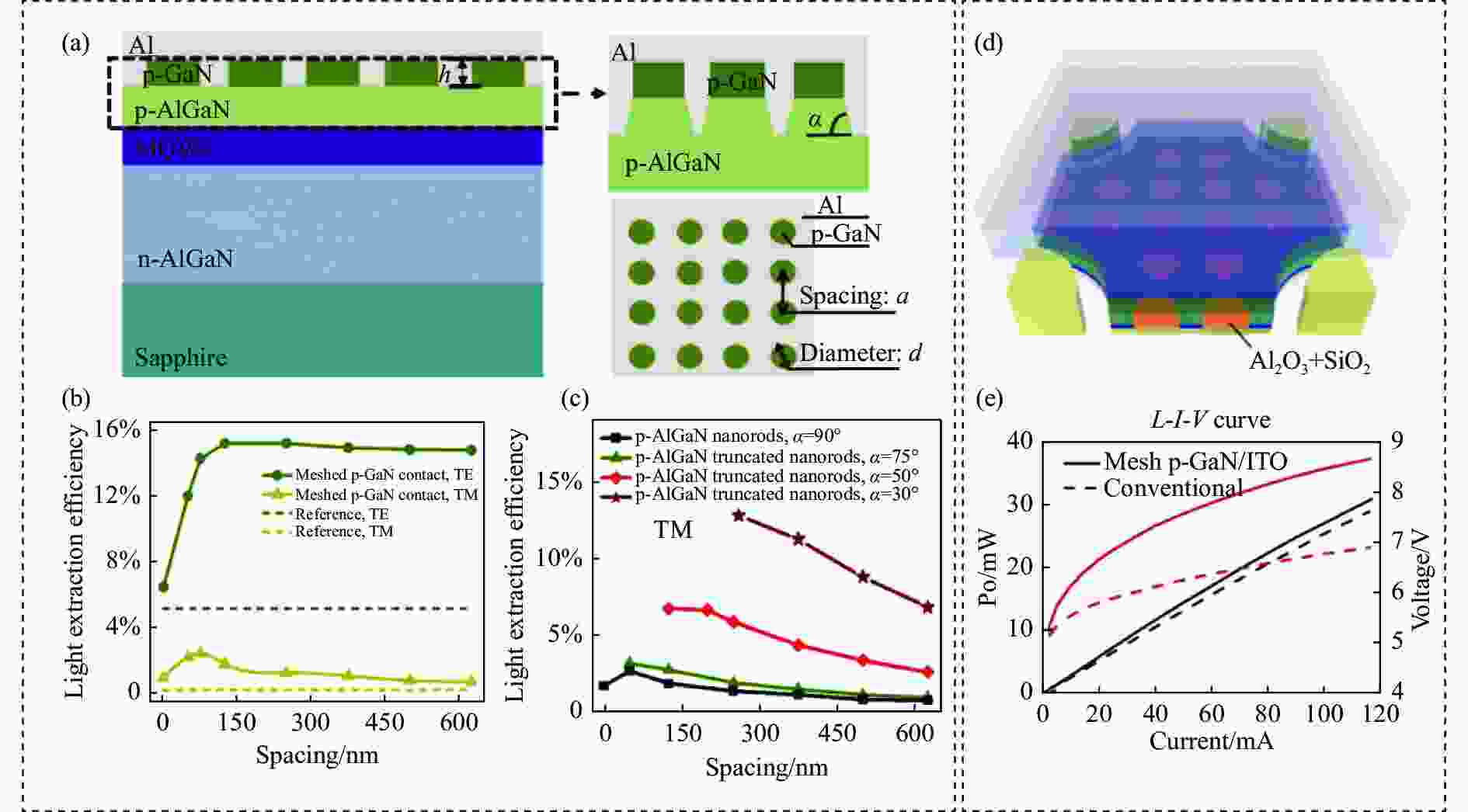
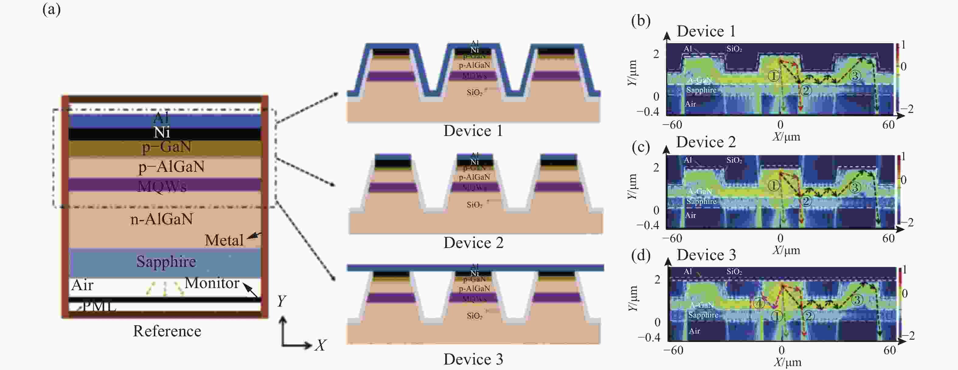
图 5 (a) 具有网状p-GaN的深紫外LED结构图;(b)具有网状p-GaN接触的DUV LED的LEE作为纳米棒间距的函数;(c) 具有网状p-GaN与截锥p-AlGaN接触的DUV LED的LEE与纳米棒间距的关系[59];(d)网状p-GaN/ITO DUV LED的示意图;(e) 两种DUV LED的L–I特性和I–V特性[60]
Figure 5. (a) Structure diagram of deep ultraviolet LED with meshed p-GaN; (b) LEEs for DUV LED with the meshed p-GaN contacts as a function of the spacing of nanorods; (c) Relationship between LEE and nanorod spacing of DUV LEDs with meshed p-GaN and truncated p-AlGaN contacts[59]; (d) Schematics of the mesh p-GaN/ITO DUV LED; (e) Measured L–I characteristics and I–V characteristics of the two kinds of DUV LEDs [60]
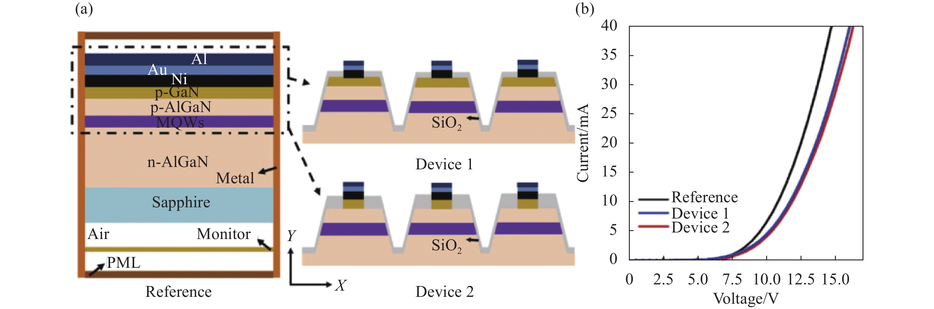
因此,在不牺牲电性能的前提下,克服p-GaN接触层的吸收是非常重要的。Fayisa等[61]选择在DUV LED上对p-GaN的中间部分进行刻蚀,该结构减少了对光子的吸收,LEE和光输出功率都得到提高,同时引入大面积的n电极面积,从而电学特性并没有恶化。当p-GaN边缘沉积电极面积不变时,p-GaN中间刻蚀面积越大,LEE越大。刻蚀面积和台面面积之比太大,会明显减少p电极的接触面积,从而使电性能变差,同时由于电流拥挤效应导致效率下降,光功率降低[62-63]。此外,Zhang等[64]结合芯片工艺,发现其电极面积必然是小于芯片面积,从而提出在DUV LED上选择刻蚀无电极覆盖的p-GaN边缘,同样制备成阵列结构,如图6(a)中的Device 2所示。图6(a)中参考器件为传统平面器件,Device 1为锥形阵列边缘未刻蚀器件。对p-GaN刻蚀后的器件,LEE和光功率同样得到了提高,这是由于对p-GaN边缘刻蚀减小光的吸收,同时产生新的逃逸光路。最关键的是对p-GaN的未被电极覆盖的部分进行蚀刻,这种结构不牺牲电极接触面积,因此在明显提高器件光提取效率时,其电学性能与Device 1是相似的,如图6(b)所示。

另外,在倒装DUV LED中,由于AlGaN与蓝宝石界面、蓝宝石与空气界面较大的折射率差值,容易在其界面发生全反射,使得大部分深紫外光子限制在器件中,最终深紫外光被器件吸收转化为热能,影响器件的发光效率。为了提升倒装DUV LED中光的散射能力且不影响P电极接触电阻,通常会在出光表面如n-AlGaN或者是蓝宝石上制备微纳结构。出光面的微纳结构能明显缓解全内反射效应,增加光的逃离角度,但其也会降低逃离锥中光的透射率。Wan等[65]研究了n-AlGaN背面粗化对不同LED结构的影响,在采用n-AlGaN表面粗化结构后,器件的小角度透射率随着入射角的增加而缓慢下降,但是大角度入射光的透过率是增加的,而粗化界面的折射率差越大,这种现象越明显。进一步研究发现,去除蓝宝石衬底的n-AlGaN表面粗化器件顶部光提取将显著增加,但由于侧壁面积减少,会导致侧壁出光率降低。Zhang等[57]也发现,如果存在比较强的p-GaN吸收,不合理的纳米图形衬底设计不仅不会增加光提取效率,还可能会使DUV LED的光提取效率变低,由于其降低了逃离锥中光的透射率。
此外,对于深紫外LED,n电极引起的光吸收问题也是非常严重。通过引入反射率更高的n电极可以有效增加光提取效率。Gao等[66]提出一种由Cr/Al金属堆叠制成的高反射n型电极,通过优化Cr的厚度来实现良好欧姆接触与高反射率的n型电极,进一步提高光提取效率。Zhang等[67]提出为了避免n电极的光吸收,而引入提高散射光的微纳结构。其使用SiO2纳米球做掩膜,对n-AlGaN进行刻蚀,形成表面微纳结构的Ga面n-AlGaN,如图7(a)所示,与传统的DUV LED相比,表面纹理Ga面n-AlGaN的DUV LED的光功率、正向电压和热特性都有了明显的改善。这是因为n-AlGaN表面微纳结构可以作为光的散射中心,使光在抵达n电极前被散射出器件,从而增强器件的光提取效率。而传统器件中的光束在n-AlGaN中无法进入逃逸锥,并不断被界面反射,最后被各种材料吸收,并转化为热量,如图7(b)所示。此外,由于n电极下的表面纹理n-AlGaN,可以有效地增加n型欧姆接触面积。因此,所提出的倒装芯片DUV LED可以降低n型欧姆接触电阻并获得更好的散热效果。而这种设计,对于深紫外μLED将会有更好的效果,由于其具有更大的n电极面积,小的芯片尺寸也会致使更多比例的光进入到n电极区域。

图 7 (a) 具有Ga面n-AlGaN纳米结构阵列的DUV LED结构图 ;(b) 传统器件(左)和表面纹理Ga面n-AlGaN器件(右)的TE偏振的XY截面电场分布[67]
Figure 7. (a) Structure diagram of DUV LED with n-AlGaN nanostructure array on Ga surface; (b) TE polarized XY cross section electric field distribution of traditional device (left) and surface finish Ga plane n-AlGaN device (right)[67]
-
近年来,被广泛研究的倾斜侧壁结构在提取深紫外LED的TM模极化光方面显示出巨大潜力。在AlGaN基DUV LED中,由于高Al含量的AlGaN材料中价带的重新排序,AlGaN多量子阱(MQW)有源区发射的深紫外光的横向磁(TM)偏振光较多[68-69]。由于TM偏振光传播方向平行于出光面,因此,与横向电场(TE)偏振光相比,TM偏振光从器件中被提取的几率更小[70]。倾斜侧壁的设计能很好地改善这个缺点,因为横向传播的TM偏振光可以经过侧壁反射到出光面逃离锥中。
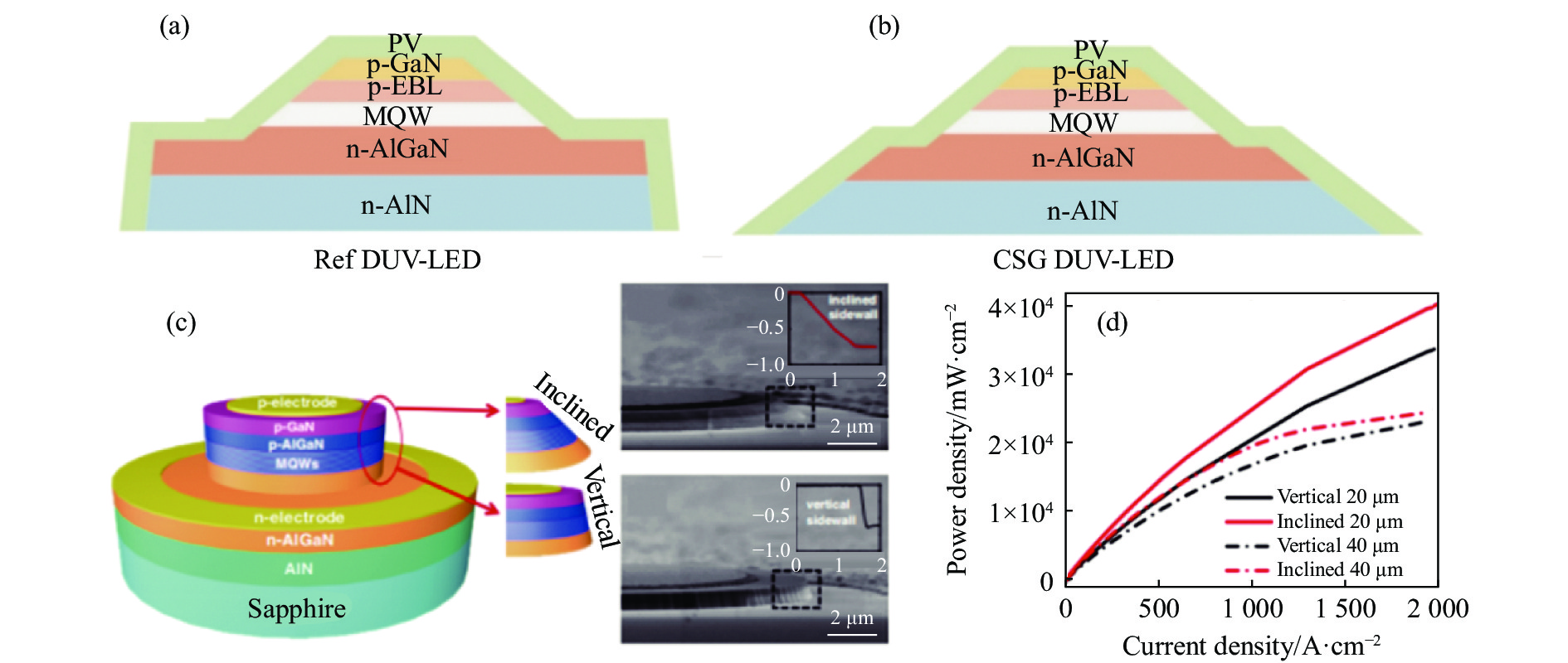
倾斜侧壁的尺寸和形状对深紫外LED的光提取有很大的影响。2014年,美国首次报道了具有金属铝全反射镜的截锥倾斜侧壁阵列的深紫外LED,并研究了三种不同尺寸倾斜侧壁散射结构的DUV LED[71]。其发现,随着偏振度的减小即TM偏振光比例的增加,倾斜侧壁结构的反射散射效果增强,这使得器件的外量子效率逐渐增强。随着倾斜侧壁结构周长的增加,LEE的改善增加,即尺寸最小的小三角形设计具有最高的EQE。这是因为它具有最小的平均散射距离,从而导致平面内光的最好散射效果,从而可以减少被p-GaN层吸收的光子。此外,Lee等[72]提出截锥形有源倾斜台面阵列相比长条形的有更好的效果,它可以以各向同性的方式有效地提取TM偏振光。 Park等发现,为了进一步的增加侧壁面积,可以把圆锥形阵列结构变成等表面积的窄条形锥形阵列,从而更有利于光的提取[73]。其也提出,对于这种小尺寸的倾斜侧壁结构,其倾斜侧壁的表面粗糙度对光提取效率也会产生显著影响。此外,侧壁刻蚀的深度对光提取效率也有较大影响,Peng等[74]研究了具有不同芯片侧壁几何形状(CSG)的DUV LED的光电性能,其CSG结构具有更深的侧壁结构,如图8(a)和(b)所示。CSG结构的倾斜外延侧壁可以比参考器件捕获更多的光子,并散射到逃离锥,从而提高器件的光提取效率。

图 8 (a) 参考DUV LED的示意图;(b) CSG DUV LED的示意图[74];(c) 具有倾斜侧壁和垂直侧壁的器件结构示意图和SEM图像;(d) 垂直和倾斜侧壁的20 µm直径的LED(实线)和40 µm直径LED (虚线)在不同电流密度下的输出功率密度[75]
Figure 8. Schematic of (a) the Ref. DUV LEDs and (b) CSG DUV LEDs [74]; (c) Schematic diagram and SEM image of device structure with inclined and vertical sidewalls; (d) Output power density under different current densities for 20 µm-diameter LEDs (solid lines) and 40 µm-diameter LEDs (dashed-dotted lines) with vertical and inclined sidewalls[75]
利用倾斜侧壁提高深紫外LED的光提取效率,其中倾斜角度的控制是非常重要。Tian等[75]研究了不同侧壁角度对UVC μLED性能的影响。相对垂直(75°)和倾斜(33°)的μLED结构如图8(c)所示。图8(d)展示倾斜侧壁与相对垂直侧壁μLED输出功率密度随电流密度的关系曲线。明显具有倾斜侧壁μLED的光功率是更大,由于引入倾斜侧壁结构增加了LEE。进一步地,他们通过FDTD仿真模拟研究发现,对于TM偏振光,侧壁角度在25°~35°的范围内时,更有利于从底部提取光。然而,当进一步减小侧壁角度,倾斜侧壁反射的光倾向于向芯片边缘传播,从而减少了从底部收集的光子总量。Chen等[70]也研究了不同倾斜侧壁角度对光功率的影响,通过FDTD模拟发现,倾斜侧壁角度在38°左右时,TM偏振光的光提取效率达到最大。此外,Zhang等[76]使用三维时域有限差分方法研究发现倾斜侧壁角度在50°左右的时候光提取效率是最大的,并利用反射逃离锥方法进行分析,得出如果只是经历一次倾斜侧壁散射的情况下,倾斜角度在46°~67°应该是最有利于倾斜侧壁利用全反射把横向传输的光直接反射到顶部逃离锥中。可以看出,倾斜侧壁角度对光提取效率影响很大,但是各个研究工作得到的最优倾斜角度并不一致,这可能与各个芯片结构有很大的关系,不同的芯片尺寸和芯片高度,都会影响最优的倾斜侧壁角度值。
除此之外,在倾斜侧壁上沉积合适的钝化层和金属,与AlGaN组成全向反射镜(ODR),可以有效提高器件的LEE和光功率[61,77]。Lee等[72]已经发现,在截锥结构的倾斜侧壁上使用具有MgF2/Al反射器,可以有效提高倾斜侧壁对深紫外光的反射。Zheng等[78]提出倾斜侧壁存在强烈的倏逝波诱导的等离子激元共振吸收。因此其提出对于介质层薄的全反射镜,应该采用大的折射率材料,而当介质层比较厚的时候,应该采用小的折射率材料。Zhang等[79]进一步提出一种远程空腔型的倾斜侧壁结构,如图9(a)所示,该结构将侧壁金属反射镜去除,移动到器件顶部。空腔结构可以很好的避免侧壁金属的光吸收,而且还可以充分利用倾斜侧壁之间的平行面作为完美的第二出光面,从而使深紫外LED的光功率提高了40%以上,如图9(d)所示。因此对于常规深紫外LED,其工作在小电流密度下,倾斜侧壁上不制备金属更有利于光提取效率。而对于DUV μLED,其工作在大电流密度下,热效应是主要矛盾,因此倾斜侧壁上的蒸镀金属会提高器件的散热性能,从而更有利于大电流密度下工作的μLED[46]。
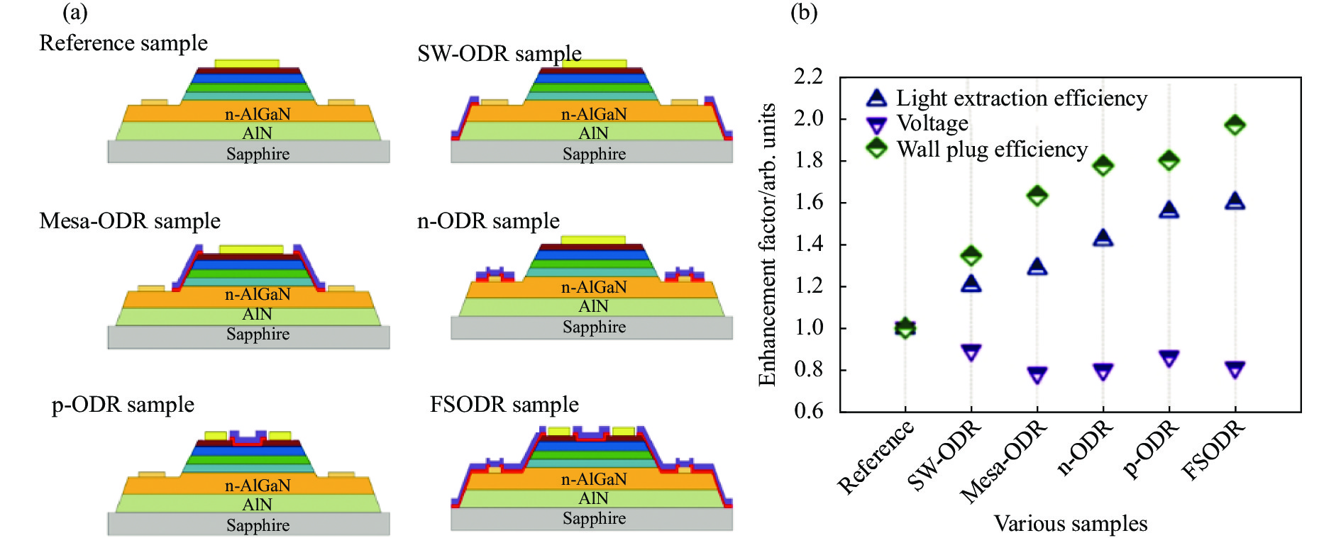
此外,Zhang等[80]提出了全空间全向反射(FSODR),此反射器覆盖在除蓝宝石表面之外的整个倒装芯片上,如图10(a)所示。图10(b)为各种ODR器件的LEE、电压以及电光转换效率(WPE)的增强因子,可以看出FSODR对器件光电学特性的提高相比任何一个单独的ODR都要大,但是单个ODR都可以为FSODR做出贡献。
-
随着器件尺寸的减小,器件侧壁表面积和台面体积的比值增加,从而有效促进了侧壁辅助所产生的热量向外辐射并能增加光提取效率[81]。但是由于DUV LED需要工作在高的工作电流密度下,且串联电阻在高电流密度下会产生更多的焦耳热,其自热效应非常严重,因此芯片温度急剧升高,从而引起LED效率的热衰减,这是DUV LED高光输出功率的关键限制。提高DUV μLED中高电流密度下的光功率,关键是提高光提取效率与解决器件的散热问题,缓解材料光吸收发热和串联电阻发热等自热效应,同时提高芯片散热特性,这对提升DUV μLED的最大光功率有着至关重要的作用。
从根本上来讲,可以降低DUV μLED器件的串联电阻来降低自热效应。器件串联电阻由接触电阻、横向扩展电阻和垂直外延电阻组成。对于DUV LED,尽管在提高掺杂效率方面已经取得了进展,但p掺杂受体的高激活能导致p-AlGaN的空穴浓度较低,从而导致高的接触电阻和外延电阻,造成显著的电流拥挤和串联电阻引起的自热问题。众所周知,电极接触电阻在串联电阻中占比很大,因此降低自热的关键还是得首先减少欧姆接触电阻率。为了实现更低的接触电阻,Srivastava等[82]建议进行等离子体处理,他们可以将接触电阻率降至5×10⁻⁴ Ω·cm2。由于金属V具有较小的电子亲和力,当使用V作为接触金属时,在具有60%AlN组成的n-AlGaN的表面上更容易形成欧姆接触。高温退火后,接触电阻率可为10−6 Ω·cm2[83]。采用V和表面等离子体处理是为了增强热离子发射和热离子辅助带内隧穿过程。与这些方法不同的是,金属-绝缘体-半导体(MIS)结构是一种非常新颖的降低欧姆接触电阻的方法,Shao等[84]提出了一种金属-绝缘体-半导体(MIS)结构,器件结构如图11(a)所示,通过制造Ti/SiO2/n-AlGaN基MIS结构来增加从金属注入到n-AlGaN的电子。SiO2中间层使得对接触金属的电子亲和力高于n-AlGaN层的导带,这有利于通过带内隧穿而不是热离子发射将电子注入n-AlGaN层,如图11(b)和(c)所示。这种设计提高了n-AlGaN层的表面电子浓度,并且有助于降低接触电阻。而在p型接触中提出一种具有p+-GaN/SiO2/ITO隧道结的DUV LED[85]。由于1 nm厚的SiO2层中隧道区宽度的减小和电场强度的增强,提高了带间隧道效率和相应的空穴注入效率,而且增强了电流扩展效应。良好的电流扩展效应显著地降低了器件的电阻率,因此降低了器件电阻,与n型MIS结构有着不同的效果。
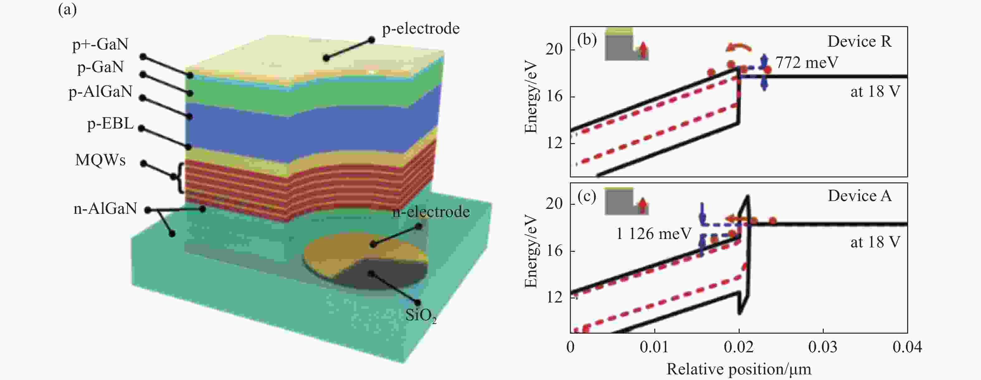
图 11 (a) MIS结构的DUV LED的示意图,即器件 A;(b) 器件 R的n-AlGaN层和n-电极金属的计算能带图;(c)器件 A的n-AlGaN层、绝缘体和n-电极金属的计算能带图[84]
Figure 11. (a) Schematic diagrams for MIS-structured DUV LED, i.e., Device A; Calculated energy band diagrams of (b) n-AlGaN layer and n-electrode metal for Device R; (c) n-AlGaN layer, insulator, and n-electrode metal for Device A[84]
降低欧姆接触电阻率,同时提高电极的反射率来减少其对深紫外光子的吸收同样重要,研究人员采取了不同的方法。Maeda等[86]发现使用高反射p型电极Ni/Al并优化Ni层厚度,可以提高EQE。他们发现最合适的Ni厚度是0.9 nm,此时EQE提高了1.8倍。但与传统Ni/Au相比,正向电压增加,这是由于Ni/Al电极与较薄Ni的接触电阻较高。为了提高Ni/Al电极的反射率,不使用较薄的Ni层,Peng等[87]利用热退火的方法,形成嵌入Al基体中的Ni团簇,从而增强了DUV LED中的光反射率,在277 nm处的反射率高达78.1%。
此外,Lee等[88]开发了一种利用电击穿实现宽带隙AlN的欧姆接触并形成ODR结构。ODR结构由p-AlGaN/Ni:AlN/Al组成,使用脉冲电击穿(PEBD)方法对AlN进行Ni掺杂,实现良好的欧姆接触,并且ODR结构反射率在250~500 nm的整个波长范围内超过90%。这是由于在电击穿时,Ni和Ga的相互扩散形成Ni3N的熔融界面。这熔融界面和Ga空位共同导致了有效的空穴传输。最近Wang等[89]提出了透明p型层和Rh/Al反射电极,由p-AlGaN梯度层和薄p-GaN接触层组成的透明p型层与Rh/Al实现良好的欧姆接触,并减少DUV光的吸收,从而减少热的产生。经过优化,Rh/Al反射型p型电极的反射率大于70%,接触电阻率为3.75×10−4 Ω·cm2。然而,对于薄p-GaN层,接触势垒高度的略微增加会增强p-GaN的耗尽,导致空穴注入效率的降低。恶化的接触降低了空穴注入效率并增加了正向电压,这导致辐射复合和WPE的下降[90]。Pan等人使用8 nm p-GaN覆盖层上的Ag纳米点形成欧姆接触,并利用Ti/Al覆盖的Ag纳米点可以防止欧姆接触的退化,保证热稳定的欧姆接触,相对于没有Ti层的器件WPE提高47.5%。因此,欧姆接触的稳定性对实现高效DUV LED的至关重要。此外,还可以通过增加欧姆接触的面积来降低接触电阻,如前文所述利用n-AlGaN粗化增加n电极接触面积,来降低欧姆接触电阻[67]。对于DUV μLED阵列,当其结区面积相同时,每个像素尺寸的减小,使阵列中μLED数量增加,制造等结面积器件所需的芯片占用面积的增加,n电极接触面积同样会增加,这两个因素会使得器件整体串联电阻降低[91]。
在保持相同芯片面积的情况下,可以利用阵列结构增加芯片的侧壁面积提高散热。Lobo Ploch等[92]对μLED阵列的研究证明与传统几何大面积LED相比,互连的DUV μLED阵列可以降低器件的串联电阻,在很大程度上缓解了电流拥挤,减少了自发热效应,从而提高了可靠性。另外,可以利用增加Al电极的面积,有效增加芯片的散热。Floyd等[91]对单个和互连的DUV μLED进行了系统的研究,并设计新的互联方式,其把整个阵列分成几个子阵列,子阵列之间有欧姆接触n电极,子阵列内部没有n电极,那么其既能保持高的光提取效率和小的欧姆接触电阻,同时保证足够小的n电极吸光,并且利用Al散热器互联每个微像素,实现更好的热扩散。当有源区面积相同时,DUV μLED阵列尺寸变小,阵列μLED的热阻抗将变小,这是因为尺寸更小使μLED电流扩展更好并且串联电阻降低[91],以及器件总表面积变大[81,92]。Zhang等[79]通过使用窄带网格几何互连的阵列空腔结构可以在很大程度上避免侧壁金属对光的损耗。虽然对于空腔型的DUV μLED其光提取效率能有效提高,但是这种设计减少了金属电极的面积,从而导致散热能力的减少。有报告比较了Al2O3/Al蒸镀前后倾斜侧壁μLED的EQE[46]。在具有侧壁金属反射镜的情况下,器件的EQE降低,这是由于侧壁反射率降低导致LEE降低的结果,但器件的效率热下降减小,并且峰值EQE位置移动到更高的电流密度,表明侧壁金属反射镜能有效改进热管理。
同时采用长条形的芯片结构,可以有效增加侧壁面积,从而提高散热特性。Park等[73]分析了具有各种台面几何形状(圆形、方形和条纹)对μLED的影响。在相同台面面积下,条纹型结构具有更大的侧壁面积,更有利于散热,同时也有利于光的提取,减少光被内部吸收而产生的热量。对侧壁刻蚀深度的加大,会增加侧壁面积,增加光提取效率,减少器件的自热效应[74]。
热的来源除了欧姆接触的焦耳加热与 LED结构中对发射光的吸收以外,还包括器件内部的非辐射复合如Shockley-Read-Hall (SRH) 、俄歇复合等引起的加热[93–95]。Deng等[96]研究了255 nm AlGaN发光二极管在温度应力作用的影响,其发现在300 K以上,光功率随温度升高而降低。但是在 300 K以下,情况相反,光功率随温度的升高而增大。在高温下有更多的缺陷被高温激活从而导致更多的陷阱辅助隧穿,增加了泄漏电流,以及靠近有源层的非辐射复合路径增加,导致效率的下降,进一步增加了热的产生。而对于μLED,虽然尺寸的减小以及阵列结构有助于散热,但其侧壁缺陷严重,会造成严重的非辐射复合与漏电流,导致效率下降,自热效应加重。因此,减少侧壁缺陷,可以有效增加器件的内量子效率并减少非辐射复合,改善热衰减。减少侧壁缺陷非辐射复合的方法包括优化热退火时间、侧壁钝化和湿法化学处理等方法,这些方法也已经在产业上经常被应用。另外,也可以通过控制载流子横向输运,从而减少侧壁缺陷的影响。关于侧壁缺陷抑制方法的研究工作已经被笔者团队做了详细的综述[15]。
-
文中工作系统综述了DUV μLED在无线光通信领域的研究现状,分析器件尺寸效应引起DUV μLED的调制特性,光提取效率,电流电压特性,光功率特性及侧壁缺陷比例变化特性及其物理机制。随着器件尺寸的减小,电流扩展效应会变得更好,可承受的电流密度增加,光功率密度也会增加。并且由于电流密度的增加,载流子复合寿命会缩短,从而提高在无线光通信应用中的调制带宽。但在大电流密度工作下的μLED热效应加剧,且台面面积变小也加大了器件的串联电阻。将μLED设计成合理的DUV μLED阵列结构会加大整体台面面积,降低串联电阻,提高散热能力以及光输出功率,但并联的阵列结构会降低带宽。采取μLED串联形式能有效地保留高的调制带宽,但自热效应会较高,效率热下降严重,无法实现输出光功率最大化。因此最重要的是提高单个DUV μLED的性能,提高LEE,减少光吸收产生的热量,改善动态电阻,同时增加散热。在器件侧壁沉积钝化层和金属会起到散热作用。此外,与传统尺寸DUV LED相比,μLED侧壁缺陷是不可忽略的。随着尺寸的减小,μLED侧壁缺陷会更加严重,导致严重的非辐射复合,降低μLED效率。目前,通过钝化层和化学处理等方法来抑制侧壁缺陷,并通过控制电流扩展来抑制侧壁缺陷引起的非辐射复合,提升μLED的效率。但在提高器件光提取效率和散热性的研究方面,仍需要投入大量的研究精力。关于 DUV μLED 器件的物理研究任重道远,仍然需要科研人员进行大量的理论分析和实践检验。
Research progress of AlGaN-based DUV μLED (invited)
-
摘要: 随着AlGaN基深紫外发光二极管(DUV LED)的发展,其不仅在杀菌消毒领域得到广泛应用,在日盲紫外光通信领域的应用也受到越来越多的关注。这主要是由于相比其他的紫外光源(如汞灯、激光),其具有功耗低、设计灵活且调制带宽高的优势。而DUV LED的带宽严重依赖于器件尺寸,器件尺寸越小,其带宽越高。但是,随着深紫外微型发光二极管(μLED)的尺寸减少,尽管其带宽得到提高,但是其光功率却急剧下降,这严重限制了深紫外μLED在光通信中的应用。文中主要总结了深紫外μLED作为日盲紫外光通信光源的研究现状和综合分析尺寸效应引起器件性能的变化及其机理;并分析出低的光提取效率和严重的自热效应是影响深紫外μLED光功率的两个主要因素。进而综述了各种提高深紫外μLED光提取效率和改善热学特性的方法。文中将为从事深紫外μLED研究的工作者提供一定的研究方向指导。
-
关键词:
- AlGaN /
- 深紫外微型发光二极管 /
- 调制带宽 /
- 光提取效率
Abstract:Significance Recently, deep-ultraviolet (DUV) communications based on DUV micro-LED technology have drawn a significant interest. This is because deep-ultraviolet (DUV) communications possess a number of advantages such as the low back-ground noise, a non-line-of-sight (NLOS) link and high security. However, its development is constrained by the lack of light sources with high power and high modulation bandwidth. In recent years, the rapid advancement of low-cost, high-output power AlGaN-based DUV LEDs has greatly accelerated the development of UVC communication and its application in various fields. Moreover, the DUV μLEDs with small chip size have the advantages of high modulation speed and low power consumption, making them attractive for implementing high-speed UVC systems. However, the low luminous efficiency of AlGaN-based μLED seriously affects the data transmission rate in deep ultraviolet communication. Therefore, we provide a review and comprehensive analysis of the size effect on the optical, electrical, thermal and modulation properties for AlGaN-based μLED, including its underlying physics mechanism. In addition, we also review various approaches to improve the light extraction efficiency and thermal characteristics of DUV μLED, which is of great significance for the study of DUV μLED. Progress Firstly, the current research status of DUV μLED as a solar blind UV communication source is introduced. The performance for UV communication system utilizing LED as a light source is summarized (Tab.1). It can be seen that under the same modulation mode, larger bandwidth and higher data transmission rate can be achieved with DUV μLED. In addition, due to the rapid attenuation of ultraviolet light power in the atmosphere, the transmission rate decreases for long distance communication. Therefore, ensuring both a large modulation bandwidth and a high optical output power for DUV μLED are very crucial for the high-speed propagation of DUV μLED optical communication system. The optical and electrical properties of DUV μLED are significantly affected by its size. The smaller size of the μLED enable them to withstand a higher current density, while the capacitance decreases as the size decreases. Consequently, the μLED with smaller size exhibits a higher modulation bandwidth. However, the reduction of the active area results in a decrease in output power as the size decreases. Additionally, the severe self-heating effect induces a thermal droop in EQE, making it challenging to achieve high power with high work currents. The low light extraction efficiency (LEE) and increased series resistor further deteriorate the self-heating effect. Therefore, to break the bottle of the light output power of μLED, it is necessary to improve the LEE, the series resistor and heat dissipation. Various micro-nano structures for nAlGaN, pAlGaN and sapphire can be used as scatter centers to improve the LEE. The patterned pAlGaN exhibits the most significant effect in improving LEE due to its proximity to the active region. However, it generally brings in a higher work voltage. Increasing the ohmic contact area and only patterning the area around the p-electrode can avoid the disadvantage. In addition, the inclined sidewall technology shows a significant potential for enhancing the LEE of DUV LED. And the shape and the sidewall reflector for the inclined sidewall have a substantial influence on the LEE of DUV μLED. Furthermore, to mitigate the self-heating effects of the device, the ohmic contact resistivity of DUV μLED device should be decreased, and the reflectivity of electrode should be increased. Therefore, the designed electrode needs to possess excellent ohmic contact and high reflectivity. Meanwhile, the device heat dissipation can be improved by increasing the electrode contact area and the device side wall area. Various technologies, such as a rectangle chip shape and a metal radiator can be utilized to enhance the device heat dissipation of DUV μLED. Conclusions and Prospects This paper presents a systematically review of the research status of DUV μLED in the field of wireless optical communication. And the size effect on the modulation characteristics, light extraction efficiency, current and voltage characteristics, optical power characteristics and side wall defect ratio are comprehensive analyzed and its underlying physical mechanism is also shown. Various technologies for improving the efficiency of light extraction and heat dissipation are summarized and discussed in detail. Although a great progress have been made in the development of DUV μLED, further research should be dedicated to enhancing the LEE and heating dissipation of DUV μLED. Especially, the electrode and the chip shape need to be designed to ensure high reflectivity and excellent ohmic contact, high efficiency scatter and good heating dissipation. -
Key words:
- AlGaN /
- DUV μLED /
- modulation bandwidth /
- light extraction efficiency
-
图 1 DUV LED器件典型的外延结构图
Figure 1. Typical epitaxial structure diagram of DUV LED devices
图 2 (a) I–V特性曲线的尺寸依赖性;(b)相同电压下电流密度的尺寸依赖性[44] ;(c) 有侧壁损伤的LED A、B、C的示意结构(LED A、B和C的可用面积比分别为85%、75%和36%[45])
Figure 2. (a) Size-dependent I–V characteristics curves; (b) Size dependence of current density under the same voltage[44]; (c) LEDs A, B, C with sidewall damages (The usable area ratios for LEDs A, B and C are 85%, 75% and 36%[45])
图 3 FDTD中模拟的TM偏振光的光提取效率与尺寸的关系
Figure 3. Relationship between light extraction efficiency and size of TM polarized light simulated in FDTD
图 4 (a)不同台面尺寸的DUV LED的光输出功率作为注入电流的函数;(b)光功率密度的尺寸依赖性[44] ;(c)三种研究器件在不同电流下的光输出功率和DUV LED的LEE增强因子(d)[52]
Figure 4. (a) Light output power as a function of injection current for the DUV LEDs with different mesa sizes; (b) Size dependence of optical power density[44] ; (c) Light output power and (d) the LEE enhancement factor of the DUV LEDs at different currents for the three investigated devices[52]
图 5 (a) 具有网状p-GaN的深紫外LED结构图;(b)具有网状p-GaN接触的DUV LED的LEE作为纳米棒间距的函数;(c) 具有网状p-GaN与截锥p-AlGaN接触的DUV LED的LEE与纳米棒间距的关系[59];(d)网状p-GaN/ITO DUV LED的示意图;(e) 两种DUV LED的L–I特性和I–V特性[60]
Figure 5. (a) Structure diagram of deep ultraviolet LED with meshed p-GaN; (b) LEEs for DUV LED with the meshed p-GaN contacts as a function of the spacing of nanorods; (c) Relationship between LEE and nanorod spacing of DUV LEDs with meshed p-GaN and truncated p-AlGaN contacts[59]; (d) Schematics of the mesh p-GaN/ITO DUV LED; (e) Measured L–I characteristics and I–V characteristics of the two kinds of DUV LEDs [60]
图 7 (a) 具有Ga面n-AlGaN纳米结构阵列的DUV LED结构图 ;(b) 传统器件(左)和表面纹理Ga面n-AlGaN器件(右)的TE偏振的XY截面电场分布[67]
Figure 7. (a) Structure diagram of DUV LED with n-AlGaN nanostructure array on Ga surface; (b) TE polarized XY cross section electric field distribution of traditional device (left) and surface finish Ga plane n-AlGaN device (right)[67]
图 8 (a) 参考DUV LED的示意图;(b) CSG DUV LED的示意图[74];(c) 具有倾斜侧壁和垂直侧壁的器件结构示意图和SEM图像;(d) 垂直和倾斜侧壁的20 µm直径的LED(实线)和40 µm直径LED (虚线)在不同电流密度下的输出功率密度[75]
Figure 8. Schematic of (a) the Ref. DUV LEDs and (b) CSG DUV LEDs [74]; (c) Schematic diagram and SEM image of device structure with inclined and vertical sidewalls; (d) Output power density under different current densities for 20 µm-diameter LEDs (solid lines) and 40 µm-diameter LEDs (dashed-dotted lines) with vertical and inclined sidewalls[75]

图 11 (a) MIS结构的DUV LED的示意图,即器件 A;(b) 器件 R的n-AlGaN层和n-电极金属的计算能带图;(c)器件 A的n-AlGaN层、绝缘体和n-电极金属的计算能带图[84]
Figure 11. (a) Schematic diagrams for MIS-structured DUV LED, i.e., Device A; Calculated energy band diagrams of (b) n-AlGaN layer and n-electrode metal for Device R; (c) n-AlGaN layer, insulator, and n-electrode metal for Device A[84]
表 1 LED作为光源时紫外通信的发展
Table 1. Development of UV communication with LED as a light source
Year Bandwidth/MHz Modulation scheme Distance/m Data rate Ref. 2022
2022
2021960
915
452OFDM
OFDM
OFDM10
17
0.56.50 Gb/s
>4 Gb/s
2 Gb/s[29]
[28]
[27]2020 170 PAM-16 1 2.4 Gb/s [30] 2020 170 PAM-16 5 1.09 Gb/s [31] 2019 438 OFDM 0.3 1.1 Gb/s [26] 2019 153 - 1.5 1.18 Gb/s [32] 2018 153 PAM-4 1.6 1.6 Gb/s [2] 2018 1.9 - 150 921.6 Kb/s [33] 2018 20 OOK - 1.92 Mb/s [34] 2017 29 OFDM - 71 Mb/s [35]  下载: 导出CSV
-
[1] Xu Z, Sadler B M. Ultraviolet communications: Potential and state-of-the-art [J]. IEEE Communications Magazine, 2008, 46(5): 67-73. doi: 10.1109/MCOM.2008.4511651 [2] Kojima K, Yoshida Y, Shiraiwa M, et al. 1.6-Gbps LED-based ultraviolet communication at 280 nm in direct sunlight[C]//2018 European Conference on Optical Communication (ECOC), 2018. [3] Guo L, Guo Y, Wang J, et al. Ultraviolet communication technique and its application [J]. Journal of Semiconductors, 2021, 42(8): 081801. doi: 10.1088/1674-4926/42/8/081801 [4] Yue Q, Li K, Kong F, et al. Analysis on the effect of amorphous photonic crystals on light extraction efficiency enhancement for GaN-based thin-film-flip-chip light-emitting diodes [J]. Optics Communications, 2016, 367: 72-79. doi: 10.1016/j.optcom.2015.12.072 [5] Krames M R, Shchekin O B, Mueller-mach R, et al. Status and future of high-power light-emitting diodes for solid-state lighting [J]. Journal of Display Technology, 2007, 3(2): 160-175. doi: 10.1109/JDT.2007.895339 [6] Kneissl M, Seong T Y, Han J, et al. The emergence and prospects of deep-ultraviolet light-emitting diode technologies [J]. Nature Photonics, 2019, 13(4): 233-244. doi: 10.1038/s41566-019-0359-9 [7] Takano T, Mino T, Sakai J, et al. Deep-ultraviolet light-emitting diodes with external quantum efficiency higher than 20% at 275 nm achieved by improving light-extraction efficiency [J]. Applied Physics Express, 2017, 10(3): 031002. doi: 10.7567/APEX.10.031002 [8] Lee D, Lee J W, Jang J, et al. Improved performance of AlGaN-based deep ultraviolet light-emitting diodes with nano-patterned AlN/sapphire substrates [J]. Applied Physics Letters, 2017, 110(19): 191103. [9] Brunner F, Protzmann H, Heuken M, et al. High-temperature growth of AlN in a production scale 11×2″ MOVPE reactor [J]. Physica Status Solidi C , 2008, 5(6): 1799-1801. [10] Nagasawa Y, Hirano A. A review of AlGaN-based deep-ultraviolet light-emitting diodes on sapphire [J]. Applied Sciences , 2018, 8(8): 1264. doi: 10.3390/app8081264 [11] Dong P, Yan J, Zhang Y, et al. AlGaN-based deep ultraviolet light-emitting diodes grown on nano-patterned sapphire substrates with significant improvement in internal quantum efficiency [J]. Journal of Crystal Growth, 2014, 395: 9-13. doi: 10.1016/j.jcrysgro.2014.02.039 [12] Maeda N, Yun J, Jo M, et al. Enhancing the light-extraction efficiency of AlGaN deep-ultraviolet light-emitting diodes using highly reflective Ni/Mg and Rh as p-type electrodes [J]. Japanese Journal of Applied Physics, 2018, 57(4S): 04FH08. doi: 10.7567/JJAP.57.04FH08 [13] Cho H K, Susilo N, Guttmann M, et al. Enhanced wall plug efficiency of AlGaN-based Deep-UV LEDs Using Mo/Al as p-Contact [J]. IEEE Photonics Technology Letters, 2020, 32(14): 891-894. [14] Tian P, McKendry J J D, Gong Z, et al. Size-dependent efficiency and efficiency droop of blue InGaN micro-light emitting diodes [J]. Applied Physics Letters, 2012, 101(23): 231110. [15] Hang S, Chuang C M, Zhang Y, et al. A review on the low external quantum efficiency and the remedies for GaN-based micro-LEDs [J]. Journal of Physics D: Applied Physics, 2021, 54(15): 153002. doi: 10.1088/1361-6463/abd9a3 [16] Hirayama H. Research status and prospects of deep ultraviolet devices [J]. Journal of Semiconductors, 2019, 40(12): 120301. [17] Chen Y, Ben J, Xu F, et al. Review on the progress of AlGaN-based ultraviolet light-emitting diodes [J]. Fundamental Research, 2021, 1(6): 717-734. doi: 10.1016/j.fmre.2021.11.005 [18] Liang S, Sun W. Recent advances in packaging technologies of AlGaN-based deep ultraviolet light-emitting diodes [J]. Advanced Materials Technologies, 2022, 7(8): 2101502. [19] Tian P, Shan X, Zhu S, et al. AlGaN ultraviolet Micro-LEDs [J]. IEEE Journal of Quantum Electronics, 2022, 58(4): 3300214. [20] Siegel A M, Shaw G A, Model J. Short-range communication with ultraviolet LEDs[C]//SPIE, 2004, 5530: 182-193. [21] Ikeda K, Horiuchi S, Tanaka T, et al. Design parameters of frequency response of GaAs-(Ga, Al) As double heterostructure LED’s for optical communications [J]. IEEE Transactions on Electron Devices, 1977, 24(7): 1001-1005. doi: 10.1109/T-ED.1977.18869 [22] Lucia M L, Hernandez-rojas J L, Leon C, et al. Capacitance measurements of p-n junctions: Depletion layer and diffusion capacitance contributions [J]. European Journal of Physics, 1993, 14(2): 86-89. doi: 10.1088/0143-0807/14/2/009 [23] Schubert E F, Hunt N E J, Malik R J, et al. Temperature and modulation characteristics of resonant-cavity light-emitting diodes [J]. Journal of Lightwave Technology, 1996, 14(7): 1721-1729. doi: 10.1109/50.507950 [24] Yang W, Zhang S, Mckendry J J D, et al. Size-dependent capacitance study on InGaN-based micro-light-emitting diodes [J]. Journal of Applied Physics, 2014, 116(4): 044512. [25] Rashidi A, Nami M, Monavarian M, et al. Differential carrier lifetime and transport effects in electrically injected III-nitride light-emitting diodes [J]. Journal of Applied Physics, 2017, 122(3): 035706. doi: 10.1063/1.4994648 [26] He X, Xie E, Islim M S, et al. 1 Gbps free-space deep-ultraviolet communications based on III-nitride micro-LEDs emitting at 262 nm [J]. Photonics Research, 2019, 7(7): B41-B47. doi: 10.1364/PRJ.7.000B41 [27] Zhu S, Qiu P, Qian Z, et al. 2 Gbps free-space ultraviolet-C communication based on a high-bandwidth micro-LED achieved with pre-equalization [J]. Optics Letters, 2021, 46(9): 2147-2150. doi: 10.1364/OL.423311 [28] MacLure D M, Xie E, Herrnsdorf J, et al. Gb/s optical wireless communications up to 17 meters using a UV-C micro-light-emitting diode[C]//2022 IEEE Photonics Conference, 2022. [29] Maclure D M, Chen C, Mckendry J J D, et al. Hundred-meter Gb/s deep ultraviolet wireless communications using AlGaN micro-LEDs [J]. Optics Express, 2022, 30(26): 46811-46821. doi: 10.1364/OE.475049 [30] Alkhazragi O, Hu F, Zou P, et al. 2.4-Gbps ultraviolet-C solar-blind communication based on probabilistically shaped DMT modulation [C]//Optical Fiber Communication Conference, 2020. [31] Alkhazragi O, Hu F, Zou P, et al. Gbit/s ultraviolet-C diffuse-line-of-sight communication based on probabilistically shaped DMT and diversity reception [J]. Optics Express, 2020, 28(7): 9111-9122. doi: 10.1364/OE.389262 [32] Yoshida Y, Kojima K, Shiraiwa M, et al. An outdoor evaluation of 1 Gbps optical wireless communication using AlGaN-based LED in 280 nm band[C]//2019 Conference on Lasers and Electro-Optics, 2019. [33] Sun Z, Zhang L, Qin Y, et al. 1 Mbps NLOS solar-blind ultraviolet communication system based on UV-LED array[C]//Proceedings SPIE, 2018, 10617: 106170O. [34] Yang Y, Chen X, You B, et al. Design of solar blind ultraviolet LED real-time video transmission system [J]. Infrared and Laser Engineering, 2018, 47(10): 1022001. (in Chinese) [35] Sun X, Zhang Z, Chaaban A, et al. 71-Mbit/s ultraviolet-B LED communication link based on 8-QAM-OFDM modulation [J]. Optics Express, 2017, 25(19): 23267-23274. doi: 10.1364/OE.25.023267 [36] Haemmer M, Roycroft B, Akhter M, et al. Size-dependent bandwidth of semipolar (1122) light-emitting-diodes [J]. IEEE Photonics Technology Letters, 2018, 30(5): 439-442. doi: 10.1109/LPT.2018.2794444 [37] Chen S W H, Huang Y M, Chang Y H, et al. High-bandwidth green semipolar (20-21) InGaN/GaN micro light-emitting diodes for visible light communication [J]. ACS Photonics, 2020, 7(8): 2228-2235. doi: 10.1021/acsphotonics.0c00764 [38] Mckendry J J D, Green R P, Kelly A E, et al. High-speed visible light communications using individual pixels in a micro light-emitting diode array [J]. IEEE Photonics Technology Letters, 2010, 22(18): 1346-1348. doi: 10.1109/LPT.2010.2056360 [39] Maclure D M, McKendry J J D, Herrnsdorf J, et al. Size-dependent characterization of deep UV micro-light-emitting diodes[C]//2020 IEEE Photonics Conference (IPC), IEEE, 2020: 1-2. [40] Qian Z, Li D, Hu F, et al. Size-dependent UV-C communication performance of AlGaN Micro-LEDs and LEDs [J]. Journal of Lightwave Technology, 2022, 40(22): 7289-7296. [41] Hu X, Liang X, Tang L, et al. Enhanced light extraction efficiency and modulation bandwidth of Deep-ultraviolet light-emitting diodes with Al nanospheres [J]. Crystals, 2022, 12(2): 289. doi: 10.3390/cryst12020289 [42] Zhang S, He R, Duo Y, et al. Plasmon-enhanced deep ultraviolet Micro-LED arrays for solar-blind communications [J]. Optics Letters, 2023, 48 (15) :3841-3844. [43] Yu H, Memon M H, Jia H, et al. Deep-ultraviolet LEDs incorporated with SiO2-based microcavities toward high-speed ultraviolet light communication [J]. Advanced Optical Materials, 2022, 10(23): 2201738. [44] Yu H, Memon M H, Wang D, et al. AlGaN-based deep ultraviolet micro-LED emitting at 275 nm [J]. Optics Letters, 2021, 46(13): 3271-3274. doi: 10.1364/OL.431933 [45] Kou J, Shen C C, Shao H, et al. Impact of the surface recombination on InGaN/GaN-based blue micro-light emitting diodes [J]. Optics Express, 2019, 27(12): A643-A653. doi: 10.1364/OE.27.00A643 [46] Floyd R, Gaevski M, Hussain K, et al. Enhanced light extraction efficiency of micropixel geometry AlGaN DUV light-emitting diodes [J]. Applied Physics Express, 2021, 14(8): 084002. [47] Guo L, Guo Y, Yang J, et al. 275 nm deep ultraviolet AlGaN-based micro-LED arrays for ultraviolet communication [J]. IEEE Photonics Journal, 2022, 14(1): 8202905. [48] Trivellin N, Monti D, De Santi C, et al. Current induced degradation study on state of the art DUV LEDs [J]. Microelectronics Reliability, 2018, 88-90: 868-872. [49] Blasco R, Ajay A, Robin E, et al. Electrical and optical properties of heavily Ge-doped AlGaN [J]. Journal of Physics D: Applied Physics, 2019, 52(12): 125101. doi: 10.1088/1361-6463/aafec2 [50] Hao G D, Taniguchi M, Tamari N, et al. Current crowding and self-heating effects in AlGaN-based flip-chip deep-ultraviolet light-emitting diodes [J]. Journal of Physics D: Applied Physics, 2018, 51(3): 035103. doi: 10.1088/1361-6463/aa9e0e [51] Shatalov M, Gong Z, Gaevski M, et al . Reliability of AlGaN-based deep UV LEDs on sapphire [C]// Proceedings SPIE, 2006, 6134: 61340P. [52] Yu H, Memon M H, Jia H, et al. A 10 × 10 deep ultraviolet light-emitting micro-LED array [J]. Journal of Semiconductors, 2022, 43(6): 062801. doi: 10.1088/1674-4926/43/6/062801 [53] Xie E, Bian R, He X, et al. Over 10 Gbps VLC for long-distance applications using a gan-based series-biased micro-LED array [J]. IEEE Photonics Technology Letters, 2020, 32(9): 499-502. doi: 10.1109/LPT.2020.2981827 [54] Jin Z, Yan L, Zhu S, et al. 10 Gbps visible light communication in 10 m free space based on violet series-biased micro-LED array and distance adaptive pre-equalization [J]. Optics Letters, 2023, 48(8): 2026-2029. doi: 10.1364/OL.487747 [55] Wang W, Lu H, Fu L, et al. Enhancement of optical polarization degree of AlGaN quantum wells by using staggered structure [J]. Optics Express, 2016, 24(16): 18176-18183. doi: 10.1364/OE.24.018176 [56] Guo Y, Zhang Y, Yan J, et al. Light extraction enhancement of AlGaN-based ultraviolet light-emitting diodes by substrate sidewall roughening [J]. Applied Physics Letters, 2017, 111(1): 011102. doi: 10.1063/1.4991664 [57] Zhang J, Chang L, Zhao Z, et al. Different scattering effect of nano-patterned sapphire substrate for TM- and TE-polarized light emitted from AlGaN-based deep ultraviolet light-emitting diodes [J]. Optical Materials Express, 2021, 11(3): 729-739. doi: 10.1364/OME.416605 [58] Zhang L, Guo Y, Yan J, et al. Deep ultraviolet light-emitting diodes based on a well-ordered AlGaN nanorod array [J]. Photonics Research, 2019, 7(9): B66-B72. doi: 10.1364/PRJ.7.000B66 [59] Zheng Y, Zhang Y, Zhang J, et al. Effects of meshed p-type contact structure on the light extraction effect for deep ultraviolet flip-chip light-emitting diodes [J]. Nanoscale Research Letters, 2019, 14: 149. [60] Kuo S Y, Chang C J, Huang Z T, et al. Improvement of light extraction in deep ultraviolet GaN light emitting diodes with mesh P-contacts [J]. Applied Sciences, 2020, 10(17): 5783. doi: 10.3390/app10175783 [61] Fayisa G B, Lee J W, Kim J, et al. Enhanced light extraction efficiency of micro-ring array AlGaN deep ultraviolet light-emitting diodes [J]. Japanese Journal of Applied Physics, 2017, 56(9): 092101. doi: 10.7567/JJAP.56.092101 [62] Lee J W, Kim D Y, Park J H, et al. An elegant route to overcome fundamentally-limited light extraction in AlGaN deep-ultraviolet light-emitting diodes: Preferential outcoupling of strong in-plane emission [J]. Scientific Reports, 2016, 6(1): 22537. doi: 10.1038/srep22537 [63] Cho J, Schubert E F, Kim J K. Efficiency droop in light-emitting diodes: Challenges and counter measures [J]. Laser and Photonics Reviews, 2013, 7(3): 408-421. doi: 10.1002/lpor.201200025 [64] Zhang G, Shao H, Zhang M, et al. Enhancing the light extraction efficiency for AlGaN-based DUV LEDs with a laterally over-etched p-GaN layer at the top of truncated cones [J]. Optics Express, 2021, 29(19): 30532-30542. doi: 10.1364/OE.435302 [65] Wan H, Zhou S, Lan S, et al. Light extraction efficiency optimization of AlGaN-based deep-ultraviolet light-emitting diodes [J]. ECS Journal of Solid State Science and Technology, 2020, 9(4): 046002. doi: 10.1149/2162-8777/ab85c0 [66] Gao Y, Chen Q, Zhang S, et al. Enhanced light extraction efficiency of AlGaN-based deep ultraviolet light-emitting diodes by incorporating high-reflective n-type electrode made of Cr/Al [J]. IEEE Transactions on Electron Devices, 2019, 66(7): 2992-2996. doi: 10.1109/TED.2019.2914487 [67] Zhang G, Wang B, Jia T, et al. Improving the performance for flip-chip AlGaN-based deep ultraviolet light-emitting diodes using surface textured Ga-face n-AlGaN [J]. Optics Express, 2022, 30(11): 17781-17788. doi: 10.1364/OE.456758 [68] Lin J Y, Jiang H X. Optical polarization in c-plane Al-rich AlN/AlxGa1-xN single quantum wells [J]. Applied Physics Letters, 2012, 101(4): 042103. [69] Nam K B, Li J, Nakarmi M L, et al. Unique optical properties of AlGaN alloys and related ultraviolet emitters [J]. Applied Physics Letters, 2004, 84(25): 5264-5266. doi: 10.1063/1.1765208 [70] Chen Q, Zhang H, Dai J, et al. Enhanced the optical power of AlGaN-based deep ultraviolet light-emitting diode by optimizing mesa sidewall angle [J]. IEEE Photonics Journal, 2018, 10(4): 6100807. [71] Wierer J J, Allerman A A, Montaño I, et al. Influence of optical polarization on the improvement of light extraction efficiency from reflective scattering structures in AlGaN ultraviolet light-emitting diodes [J]. Applied Physics Letters, 2014, 105(6): 061106. [72] Lee J W, Park J H, Kim D Y, et al. Arrays of truncated cone AlGaN deep-ultraviolet light-emitting diodes facilitating efficient outcoupling of in-plane emission [J]. ACS Photonics, 2016, 3(11): 2030-2034. doi: 10.1021/acsphotonics.6b00572 [73] Park J H, Pristovsek M, Cai W, et al. Interplay of sidewall damage and light extraction efficiency of micro-LEDs [J]. Optics Letters, 2022, 47(9): 2250-2253. doi: 10.1364/OL.456993 [74] Peng K W, Tseng M C, Lin S H, et al. Sidewall geometric effect on the performance of AlGaN-based deep-ultraviolet light-emitting diodes [J]. Optics Express, 2022, 30(26): 47792-47800. doi: 10.1364/OE.475219 [75] Tian M, Yu H, Memon M H, et al. Enhanced light extraction of the deep-ultraviolet micro-LED via rational design of chip sidewall [J]. Optics Letters, 2021, 46(19): 4809-4812. doi: 10.1364/OL.441285 [76] Zhang Y, Meng R, Zhang Z H, et al. Effects of inclined sidewall structure with bottom metal air cavity on the light extraction efficiency for AlGaN-based deep ultraviolet light-emitting diodes [J]. IEEE Photonics Journal, 2012, 10(4): 8200809. [77] Guo Y, Zhang Y, Yan J, et al. Enhancement of light extraction on AlGaN-based deep-ultraviolet light-emitting diodes using a sidewall reflection method[C]//2016 13th China International Forum on Solid State Lighting: International Forum on Wide Bandgap Semiconductors China (SSLChina: IFWS), IEEE, 2016: 127-130. [78] Zheng Y, Zhang J, Chang L, et al. Understanding omni-directional reflectors and nominating more dielectric materials for deep ultraviolet light-emitting diodes with inclined sidewalls [J]. Journal of Applied Physics, 2020, 128(9): 093106. [79] Zhang J, Chang L, Zheng Y, et al. Integrating remote reflector and air cavity into inclined sidewalls to enhance the light extraction efficiency for AlGaN-based DUV LEDs [J]. Optics Express, 2020, 28(11): 17035-17046. doi: 10.1364/OE.393166 [80] Zhang S, Liu Y, Zhang J, et al. Optical polarization characteristics and light extraction behavior of deep-ultraviolet LED flip-chip with full-spatial omnidirectional reflector system [J]. Optics Express, 2019, 27(20): A1601-A1614. doi: 10.1364/OE.27.0A1601 [81] Chen H S, Yeh D M, Lu C F, et al. Mesa-size-dependent color contrast in flip-chip blue/green two-color InGaN/GaN multi-quantum-well micro-light-emitting diodes [J]. Applied Physics Letters, 2006, 89(9): 093501. [82] Srivastava S, Hwang S M, Islam M, et al. Ohmic contact to high-aluminum-content AlGaN epilayers [J]. Journal of Electronic Materials, 2009, 38(11): 2348-2352. doi: 10.1007/s11664-009-0924-y [83] Haidet B B, Sarkar B, Reddy P, et al. Nonlinear analysis of vanadium- and titanium-based contacts to Al-rich n-AlGaN [J]. Japanese Journal of Applied Physics, 2017, 56(10): 100302. doi: 10.7567/JJAP.56.100302 [84] Shao H, Che J, Chu C, et al. On the impact of a metal-insulator-semiconductor structured n-electrode for AlGaN-based DUV LEDs [J]. Applied Optics, 2021, 60(36): 11222-11226. doi: 10.1364/AO.446613 [85] Che J, Shao H, Chu C, et al. Enhanced performance of an AlGaN-based deep ultraviolet light-emitting diode using a p+-GaN/SiO2/ITO tunnel junction [J]. Optics Letters, 2022, 47(4): 798-801. doi: 10.1364/OL.448632 [86] Maeda N, Jo M, Hirayama H. Improving the efficiency of AlGaN Deep-UV LEDs by using highly reflective Ni/Al p-type electrodes [J]. Physica Status Solidi A, 2018, 8(2): 1901430. [87] Peng X, Guo W, Xu H, et al. Significantly boosted external quantum efficiency of AlGaN-based DUV-LED utilizing thermal annealed Ni/Al reflective electrodes [J]. Applied Physics Express, 2021, 14(7): 072005. doi: 10.35848/1882-0786/ac0b07 [88] Lee T H, Park T H, Shin H W, et al. Smart wide-bandgap omnidirectional reflector as an effective hole-injection electrode for deep-UV light-emitting diodes [J]. Advanced Optical Materials, 2020, 8(2): 1901430. [89] Wang L, Xu F, Lang J, et al. Transparent p-type layer with highly reflective Rh/Al p-type electrodes for improving the performance of AlGaN-based deep-ultraviolet light-emitting diodes [J]. Japanese Journal of Applied Physics, 2023, 62(3): 030904. doi: 10.35848/1347-4065/acbf14 [90] Pan S, Chen K, Guo Y, et al. Enhancement of the light output efficiency and thermal stability of AlGaN-based deep-ultraviolet light-emitting diodes with Ag-nanodot-based p-contacts and an 8-nm p-GaN cap layer [J]. Optics Express, 2022, 30(25): 44933-44942. doi: 10.1364/OE.476103 [91] Floyd R, Gaevski M, Alam M D, et al. An opto-thermal study of high brightness 280 nm emission AlGaN micropixel light-emitting diode arrays [J]. Applied Physics Express, 2021, 14(1): 014002. [92] Lobo Ploch N, Rodriguez H, Stolmacker C, et al. Effective thermal management in ultraviolet light-emitting diodes with micro-LED arrays [J]. IEEE Transactions on Electron Devices, 2013, 60(2): 782-786. doi: 10.1109/TED.2012.2234462 [93] Sun W, Shatalov M, Deng J, et al. Efficiency droop in 245-247 nm AlGaN light-emitting diodes with continuous wave 2 mW output power [J]. Applied Physics Letters, 2010, 96(6): 061102. [94] De Santi C, Meneghini M, Monti D, et al. Recombination mechanisms and thermal droop in AlGaN-based UV-B LEDs [J]. Photonics Research, 2017, 5(2): A44-A51. doi: 10.1364/PRJ.5.000A44 [95] Meneghini M, De Santi C, Tibaldi A, et al. Thermal droop in III-nitride based light-emitting diodes: Physical origin and perspectives [J]. Journal of Applied Physics, 2020, 127(21): 211102. doi: 10.1063/5.0005874 [96] Deng S, Chen Z, Li M, et al. Variable temperature thermal droop characteristics of 255 nm UV LED [J]. Applied Physics Letters, 2022, 121(3): 031104. -

 点击查看大图

计量
- 文章访问数: 295
- HTML全文浏览量: 71
- PDF下载量: 55
- 被引次数: 0

