


 下载:
下载:


-
硅材料具有储量丰富、成本较低和光学性能优异的优点[1],随着微电子工艺技术的不断发展,硅基器件被广泛应用在光伏电池[2−3]、光通信[4−5]和光电探测[6]等领域。硅基光电探测器在可见光波段的应用已经趋于成熟,但由于硅的禁带宽度为1.12 eV,硅的光电响应截止波长约为1100 nm,单纯的硅不能作为近红外光电探测器的材料[7]。制备具有近红外波段探测能力的单元器件主要利用例如锗[8]、锗硅[9]、砷化铟镓[10−11]以及磷化铟[12]等半导体材料,但这些非硅材料的光电探测器成本高,且难以与硅驱动的电路集成。
近年来随着纳米加工技术和等离激元光学的发展,纳米金属结构常被用来增强硅基器件的近红外吸收。例如,2022年,Syu等[13]成功地研究了Ag/n-Si肖特基光电探测器,Si基光电检测器的光电探测极限从1 100 nm延伸到1 670 nm。同年,Li等[14]提出了一种以钨为金属层、氧化铝为绝缘层的纳米环形圆柱阵列天线。该天线在可见光和近红外光的宽带吸收范围内具有96.93%的平均吸收效率。同年,Brahim等[15]通过电子束蒸发沉积的Ag薄膜的简单脱湿和退火工艺,形成不同表面密度的Ag-NPs网络。这些Ag网络被用作c-Si太阳能电池的宽带等离子体界面,产生高达50%的光电流增强。以上结果表明,纳米金属结构可以增强硅对近红外光的吸收,但是鲜有提到不同浓度的纳米金属结构组合起来对于吸收效果的影响。
文中设计了一种硅基的、纳米金属粒子梯度掺杂的近红外波段吸收增强薄膜。通过等效介质理论计算了不同浓度下掺杂层的介电常数,模拟计算了薄膜在不同波长下的吸收率。结果表明:该设计可以有效提高硅的近红外波段吸收率,提升效果最高可达到10.7 dB。
-
在按照需求设计具有特定功能的复合介质时,常使用等效介质理论来快速计算复合介质的等效电磁参数[16],这种方式大大提高了整个设计流程的效率。等效介质理论的思想是,当电介质中的掺杂物大小远小于入射波的波长,该复合材料就可以从宏观的角度分析其电磁特性,此时可以用准静态来近似[17]。
当电介质中掺杂物的含量较低,微粒间的相互作用和更高的多级作用可以忽略,此时通常采用Maxwell-Garnett理论(下面简称M-G)来计算复合介质的等效电磁参数[18]。另外,参考文献[19]实验证明了M-G模型在填充因子低于5%情况下的可靠性。如果设掺杂物为半径为$R$的球形,介电常数为${\varepsilon _m}$,根据Clausius-Mossotti公式可知,在由微粒和介质构成的二元体系下,微粒的电极化度$\alpha $与材料宏观介电常数${\varepsilon _e}$之间的关系为[20]:
$$ \frac{{{\varepsilon _e} - {\varepsilon _h}}}{{{\varepsilon _e} + 2{\varepsilon _h}}} = \frac{{n\alpha }}{{3{\varepsilon _0}}} $$ (1) 式中:$n$表示单位体积内的粒子数目;${\varepsilon _h}$表示电介质的介电常数。其中电极化度为:
$$ \alpha = 4\pi {\varepsilon _0}{R^3}\frac{{{\varepsilon _m} - {\varepsilon _h}}}{{{\varepsilon _m} + 2{\varepsilon _h}}} $$ (2) 将公式(2)代入公式(1),得:
$$ \frac{{{\varepsilon _e} - {\varepsilon _h}}}{{{\varepsilon _e} + 2{\varepsilon _h}}} = p\frac{{{\varepsilon _m} - {\varepsilon _h}}}{{{\varepsilon _m} + 2{\varepsilon _h}}} $$ (3) 这就是M-G等效介质公式,其中,$p$为掺杂物所占的体积分数。
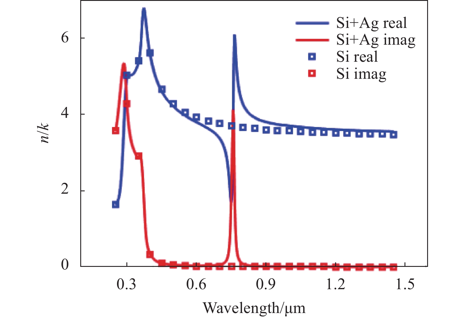
根据银和金的折射率实验数据,可以拟合出它们的折射率曲线,如图1所示(图中点表示实验数据,线表示拟合结果)。然后,利用关系$\varepsilon {\text{ = }}{n^2}$,可以得到两种金属的介电常数[21]。接下来将纳米银粒子的体积分数(以1%为例)、介电常数以及硅的介电常数分别代入公式(3),可以得到Si掺杂Ag复合介质在可见光和近红外波段的等效介电常数。最后,将结果转换为复折射率,并与介质硅的复折射率进行对比,如图2所示。从图中可以看出,两者的主要区别为760 nm附近的波段范围,说明掺杂物对于复合介质电磁性能的影响主要发生在这个波段。掺杂对于复折射率实部的影响是,会在750 nm附近出现值剧烈的折射率变化,产生一个极大和一个极小值。掺杂对于复折射率虚部的影响是,会在760 nm附近产生一个峰值。出现该情况的原因如下,将公式(3)转变为:
$$ {\varepsilon _e} = {\varepsilon _h}\left[ {1 - \frac{p}{{{{{\varepsilon _h}} \mathord{\left/ {\vphantom {{{\varepsilon _h}} {\left( {{\varepsilon _h} - {\varepsilon _m}} \right)}}} \right. } {\left( {{\varepsilon _h} - {\varepsilon _m}} \right)}} - \frac{1}{3}\left( {1 - p} \right)}}} \right] $$ (4) 
图 1 金属的复折射率与拟合曲线。(a) 银的折射率;(b) 金的折射率
Figure 1. Complex refractive index and fitting curve of metals. (a) Refractive index of silver; (b) Refractive index of gold

图 2 Si掺杂Ag复合材料和硅的复折射率
Figure 2. Complex refractive index of composite materials and silicon
当$ {{{\varepsilon _h}} \mathord{\left/ {\vphantom {{{\varepsilon _h}} {\left( {{\varepsilon _h} - {\varepsilon _m}} \right)}}} \right. } {\left( {{\varepsilon _h} - {\varepsilon _m}} \right)}} $的实部取(0,1)之间时,分母可能会消失,而此时$ {{{\varepsilon _h}} \mathord{\left/ {\vphantom {{{\varepsilon _h}} {\left( {{\varepsilon _h} - {\varepsilon _m}} \right)}}} \right. } {\left( {{\varepsilon _h} - {\varepsilon _m}} \right)}} $的虚部保持有限。这种情况称为几何共振,由复合材料的微观几何和组分的介电系数决定[17]。
-
参考文献[22]中的结构,设计一种总厚度为1 000 nm复合硅层,其中硅层被等分为20层,每层纳米金属粒子的掺杂浓度从0.25%开始以0.25%为梯度均匀增加直到5%,或从5%开始以0.25%为梯度均匀减少直到0.25%。选择银和金两种纳米金属粒子进行掺杂。结构示意图如图3所示(其中,(a)为浓度递增掺杂结构;(b)为浓度递减掺杂结构),示意图分别给出了顶部、中部和底部掺杂层,对其他掺杂层进行了适当的省略。

图 3 梯度掺杂材料的结构示意图。
Figure 3. Structural schematic diagram of gradient doped materials
根据等效介质理论计算出复合介质的等效介电常数,利用关系$n = \sqrt \varepsilon $得到等效折射率,就可以使用介质的等效折射率计算复合介质的吸收率。图4为不同掺杂浓度下复合介质的等效折射率。可以看出,与未掺杂的介质硅相比,掺杂浓度越高,760 nm波长附近的介质等效折射率变化越明显。

图 4 不同掺杂浓度的介质的等效折射率。(a) 复折射率实部;(b) 复折射率虚部
Figure 4. Equivalent refractive index of media with different doping concentrations. (a) Real part of complex refractive index; (b) Imaginary part of complex refractive index
使用时域有限差分法(FDTD)来模拟计算复合介质在可见光和近红外波段的吸收。这里采用两种掺杂的方式,一种是从顶层开始掺杂浓度逐渐下降,另一种是从顶层开始掺杂浓度逐渐提升。仿真设置如图5所示。为了减少仿真时间,仿真区域设置为2D,如方框所示。上下的边界设置为PML边界,左右边界设置为Periodic边界,为了避免产生掺杂层厚度导致的法布里-珀罗谐振,将最后一层掺杂层延伸到仿真区域底部的边界以外。另外三个平行平面从上到下分别代表反射监视器、光源、透射监视器。其中光源选择垂直入射的平面波。

图 5 仿真模型示意图
Figure 5. Schematic diagram of simulation model
-
硅基梯度掺杂结构的设计可以从两个方面进行考虑,一是对比不同掺杂方式的吸收提升效果,二是纳米金属粒子的选择。通过对仿真结果进行分析,从而得到最优解。选用梯度缓慢变化的掺杂方式是为了避免纳米粒子掺杂浓度过大引起折射率的变化,因为较大的浓度梯度会引起反射率的突变。在超材料的设计中,常选用金和银两种贵金属,将它们应用在可见光和红外波段往往会带来优异的性能。
-
首先选择纳米银粒子作为掺杂粒子。图6展示了纳米银粒子掺杂浓度递减、纳米银粒子掺杂浓度递增和未掺杂三种情况下复合介质的反射率、透射率和吸收率曲线。如图6(a)所示,递增掺杂对反射率的影响很小,仅在755 nm附近产生微小的波动。但递减掺杂的情况下,反射率产生很大的波动,在710 nm处存在一个极小值0.05,在760 nm处存在极大值0.9。图中同样给出了掺杂浓度为5%和0.25%下介质复折射率的实部曲线,可以看出在430~1450 nm范围内,递减掺杂方式下的反射率曲线和掺杂浓度为5%的掺杂层的等效折射率曲线类似,在680~830 nm范围内,递增掺杂方式下的反射率曲线和掺杂浓度为0.25%的掺杂层的等效折射率曲线类似,表明反射率曲线的变化与复折射率实部的变化有关。反射发生在空气和顶层以及相邻层之间的界面上,而相邻层因为折射率相近,反射可以忽略。递减掺杂的情况下,顶层介质的掺杂浓度为5%,折射率实部相比于硅有较大的变化,所以反射率曲线也会随着折射率实部的变化趋势而发生较大的改变。相比而言,递增掺杂的情况下顶层的掺杂浓度为0.25%,折射率实部相比于硅只存在很小的变化,所以反射率曲线只会在折射率实部发生变化的波段范围产生微小的改变。另外,将复合介质设计成掺杂浓度缓慢变化的原因,是为了避免较大的折射率梯度导致强烈的反射。

图 6 纳米银粒子掺杂材料的模拟吸收谱。(a) 反射率;(b) 透射率;(c) 吸收率;(d) 吸收提升效果
Figure 6. Simulated absorption spectra of silver nanoparticles doped materials. (a) Reflectivity; (b) Transmissivity; (c) Absorptivity; (d) Absorption improvement effect
如图6(b)所示,在纳米银粒子递增掺杂方式下,复合介质可以在640~1 110 nm波段范围内降低透射率;在递减掺杂方式下,可以在660~1 450 nm波段范围内降低透射率。另外,两种掺杂方式均可实现720~800 nm波段范围内透射率几乎为0。图中同样给出了掺杂浓度为5%和0.25%下介质复折射率的虚部曲线,可以看出:掺杂浓度为5%的介质折射率虚部的曲线相比于硅的变化范围和透射率为0的范围一致,并且两种掺杂方式下透射率为0的范围相同。这是因为折射率的虚部代表介质对电磁波的吸收能力,掺杂导致介质折射率的虚部曲线在720~800 nm波段范围内出现峰值,介质该波段内的吸收能力增强,并且掺杂浓度越大导致折射率虚部曲线峰值越大,
复合介质的吸收能力越强。梯度掺杂的复合介质吸收能力的增强程度由最大掺杂浓度决定,两种掺杂方式的最大掺杂浓度都为5%,所以,两种掺杂方式下复合介质吸收能力的增强程度一样,都可以在720~800 nm波段范围内实现0透射。而540~670 nm和840~1450 nm波段范围内两种掺杂方式下透射率的区别,主要是由该波段内反射率的差异造成的。
根据前面得到的反射率和透射率曲线,可以通过关系$A = 1 - R - T$得到复合材料的吸收率曲线,如图6(c)所示。在640~1080 nm波段范围内,两种掺杂方式都可以增强介质的吸收,但递减掺杂的情况下,吸收率曲线出现差别较大的极大值和极小值,影响该波段范围内吸收率的总体提升效果。两种掺杂方式下,在640~1080 nm波段内都存在两个吸收峰,原因如下:由于两种掺杂方式下的纳米金属粒子的最大浓度和浓度梯度相同,两种结构的吸收能力相似,在不考虑反射率的情况下,吸收率会在770 nm出现吸收单峰。而由前文介绍的几何共振原理可知,纳米金属粒子的掺杂改变了硅材料的介电特性,具体表现为表层的反射率在波长750 nm附近出现一个Fano共振的形式。介质层吸收的是未被表层反射的剩余电磁波,所以,最终吸收的电磁波总量会受到表层反射的影响。造成的结果就是,反射率曲线中的Fano共振会导致吸收率原本的单峰分裂为两峰。递减掺杂下波长709 nm处的吸收峰高于递增掺杂,是因为该波长下的反射率较小,更多的光进入到结构中被吸收。递减掺杂下波长804 nm处的吸收峰低于递增掺杂,是因为该波长下的反射率较大,更多的光被反射掉而无法被结构吸收。
按照如下公式$ 10{\mathrm{log}}_{10}({A}_{2}/{A}_{1}) $(其中${A_1}$、${A_2}$分别代表未掺杂介质吸收率和掺杂介质吸收率)计算两种掺杂方式对吸收率的提升效果,计算结果如图6(d)所示。相比之下,递增掺杂的吸收提升效果更好,峰值为8.4 dB,而递减掺杂在750 nm处存在一个极小值0 dB。
-
选择吸收效果较优的递增掺杂方式(下文提到的掺杂均为递增掺杂),对比不同纳米金属粒子掺杂对介质反射率、透射率和吸收率的影响,如图7所示。从图7(a)可以看出,两种情况下的反射率差别不大,只是发生波动的范围不同,纳米银粒子掺杂下介质发生波动的范围在755 nm附近,金在820 nm附近,纳米金粒子掺杂下的介质反射率曲线发生波动的波长略大于银。图中同样给出了两种纳米金属粒子掺杂(掺杂浓度为0.25%)介质的复折射率实部曲线,可以看出反射率曲线发生波动的位置与折射率实部曲线发生波动的位置具有一致性,说明掺杂的金属种类对折射率实部具有很小的影响,所以导致反射率也没有发生明显的变化。

图 7 不同纳米金属粒子掺杂材料的模拟吸收谱。(a) 反射率;(b) 透射率;(c) 吸收率;(d) 吸收提升效果
Figure 7. Simulated absorption spectra of materials doped with different nano metal particles. (a) Reflectivity; (b) Transmissivity; (c) Absorptivity; (d) Absorption improvement effect
由图7(b)可以看出,纳米银粒子掺杂可以在636~1120 nm范围内降低透射率,纳米金粒子掺杂可以在610~1450 nm范围内降低透射率,具有更宽的减透波段范围。另外,两种情况下的透射率为0的波段也不同,纳米银粒子掺杂可以实现在720~792 nm范围内透射率为0,纳米金粒子掺杂可实现783~892 nm波段内透射率为0。同样图中给出了两种纳米金属粒子掺杂介质(掺杂浓度为5%)的折射率虚部曲线,可以看出纳米金属粒子的不同导致折射率虚部发生变化的波段不同,纳米金粒子对介质折射率虚部产生影响的波长和波长范围都要大于银。另外折射率虚部曲线峰值附近大于0的波段与透射率为0的波段重合,说明不同纳米金属粒子通过影响介质的折射率虚部来对介质的透射率产生影响。
计算得到两种情况下的吸收率曲线,见图7(c)。纳米金粒子掺杂可在更宽的波段610~1450 nm内增强吸收,而纳米银粒子掺杂仅在640~1080 nm波段范围内增强吸收。从前面的分析可知,增强吸收的原理主要是纳米金属粒子掺杂降低了材料的透射率,并且掺杂造成反射率曲线的波动导致了吸收率峰值处的波动。另外纳米金粒子对介质产生影响的波长要大于银,影响的波段范围也大于银,所以金对于介质吸收率的提升效果要优于银。图7(d)对比不同纳米金属粒子的吸收提升效果,可以明显看到纳米金粒子的吸收提升波段更宽,吸收提升峰值也更大,可以达到10.4 dB,对于近红外波段有着更优的吸收提升效果。
-
文中基于等效介质理论,设计了一种纳米金属粒子梯度掺杂的复合材料,通过时域有限差分方法对复合材料的电磁效果进行仿真模拟,得到了复合材料在可见光和近红外波段的反射率、透射率和吸收率曲线。通过改变掺杂方式与金属材料的选择,总结出不同掺杂方式和纳米金属粒子对介质电磁特性的影响。其中效果最优的是纳米金粒子递增掺杂,可以有效提高硅基材料610~1450 nm波段的电磁波吸收效率,提升效果最高可达到10.7 dB。
Silicon based near-infrared absorption enhancement structure with gradient doping of nano metal particles
-
摘要: 硅基光电子与CMOS工艺兼容,借助成熟的微电子加工工艺平台可以实现大规模批量生产,具有低成本、高集成度、高可靠性的优势。其中,硅基半导体探测器是目前应用最为广泛的可见光波段探测设备,将其工作频段拓展到近红外波段具有重要意义。由于硅的禁带宽度,硅基材料在近红外波段电磁波吸收存在明显限制,硅基探测器在近红外波段的应用受到挑战。根据纳米金属粒子发生局域表面等离子共振时产生的近场增强效应,提出了一种纳米金属粒子梯度掺杂的硅基结构。通过应用等效介质理论,模拟了复合硅基结构在可见光与近红外波段的吸收特性。结果表明:该结构在近红外波段具有电磁波吸收提升效果,并且当选择纳米金粒子梯度递增掺杂时,可以在610~1450 nm波段提升吸收性能,最高提升可达到10.7 dB。所提出的结构可以有效增强硅基材料在近红外波段的吸收效率,研究结果为硅基半导体探测器在近红外波段的应用提供了重要参考。Abstract:
Objective Silicon based optoelectronics are compatible with CMOS technology, and with the help of mature microelectronic processing platforms, large-scale mass production can be achieved. It has the advantages of low cost, high integration, and high reliability. Among them, the application of silicon based semiconductor detectors in the visible light band has become more mature. However, the commonly used semiconductor materials for near-infrared band detectors have drawbacks such as difficulties in compatibility with existing CMOS processes and high prices. Therefore, expanding the operating frequency range of silicon based semiconductor detectors to the near-infrared band is of great significance. Due to the bandgap width of silicon, there are significant limitations in the absorption of electromagnetic waves by silicon based materials in the near-infrared band, posing serious challenges for the application of silicon based detectors in the near-infrared band. Methods In order to break through the bandgap width limitation of silicon and improve the absorption performance of silicon materials in the near-infrared band, a silicon based structure based on gradient doping of nanometallic particles was proposed, based on the near-field enhancement effect generated by local surface plasmon resonance of nanometallic particles. The slow change in doping concentration can effectively solve the severe change in reflectivity caused by refractive index mutation. By applying the Maxwell Garnett equivalent medium theory, the absorption characteristics of composite silicon based structures in the visible and near-infrared bands were simulated, and the effects of two doping concentration changes and two doping metals on the absorption enhancement effect of silicon based materials were compared. Results and Discussions The results indicate that the structure has a significant improvement in electromagnetic wave absorption in the near-infrared band. When the doped metal is silver, both decreasing and increasing doping can bring absorption improvement in the 640-1080 nm wavelength range. However, increasing doping can avoid the drastic change in reflectivity caused by refractive index mutations, and its effect is significantly better than decreasing doping(Fig.6). When comparing the effects of different metals, the absorption enhancement band brought by the doping of gold nanoparticles is wider than that of silver nanoparticles. So when choosing gradient increasing doping of gold nanoparticles, the effect is optimal, and the absorption performance can be improved in the 610-1450 nm wavelength range, with a maximum improvement of 10.7 dB(Fig.7). Conclusions A silicon based structure that can break through the bandgap width limitation of silicon was proposed, near-infrared absorption enhancement was achieved, and the absorption enhancement effect under different conditions was simulated and analyzed. The proposed structure can effectively enhance the absorption efficiency of silicon based materials in the near-infrared band, which helps to improve the performance of silicon based devices. And by comparing different doping methods and metal selection, it is concluded that gradient increasing doping of gold nanoparticles is the optimal choice. The research results of this article provide important references for the application of silicon based semiconductor detectors in the near-infrared band. -
图 1 金属的复折射率与拟合曲线。(a) 银的折射率;(b) 金的折射率
Figure 1. Complex refractive index and fitting curve of metals. (a) Refractive index of silver; (b) Refractive index of gold
图 2 Si掺杂Ag复合材料和硅的复折射率
Figure 2. Complex refractive index of composite materials and silicon
图 4 不同掺杂浓度的介质的等效折射率。(a) 复折射率实部;(b) 复折射率虚部
Figure 4. Equivalent refractive index of media with different doping concentrations. (a) Real part of complex refractive index; (b) Imaginary part of complex refractive index
图 6 纳米银粒子掺杂材料的模拟吸收谱。(a) 反射率;(b) 透射率;(c) 吸收率;(d) 吸收提升效果
Figure 6. Simulated absorption spectra of silver nanoparticles doped materials. (a) Reflectivity; (b) Transmissivity; (c) Absorptivity; (d) Absorption improvement effect
-
[1] 杨柳, 蒋世磊, 孙国斌等 . 等离激元增强金属-硅组合微结构近红外吸收 [J]. 光学学报,2020 ,40 (21 ):162 -168 . Yang Liu, Jiang Shilei, Sun Guobin, et al. Plasmonic enhanced near-infrared absorption of metal-silicon composite microstructure [J]. Acta Optica Sinica, 2020, 40(21): 2124003. (in Chinese)[2] Banerjee S, Das M K. A review of Al2O3 as surface passivation material with relevant process technologies on c-Si solar cell [J]. Optical and Quantum Electronics, 2021, 53(1): 1-25. doi: 10.1007/s11082-020-02634-9 [3] Sundarapura P, Zhang X M, Yogai R, et al. Nanostructure of porous Si and Anodic SiO2 surface passivation for improved efficiency porous Si solar cells [J]. Nanomaterials, 2023, 11(2): 459. [4] 李欣, 李芸, 王徐等 . 面向可见光通信的硅基InGaN/GaN多量子阱波导定向耦合器光子集成芯片 [J]. 电子与信息学报,2022 ,44 (8 ):2695 -2702 . doi: 10.11999/JEIT210758 Li Xin, Li Yun, Wang Xu, et al. Silicon-based InGaN/GaN multiple quantum well waveguide directional coupler photonic integrated chip for visible light communication [J]. Journal of Electronics & Information Technology, 2022, 44(8): 2695-2702. (in Chinese) doi: 10.11999/JEIT210758[5] Sharma A K , Pandey A K. Metal oxide grating based plasmonic refractive index sensor with Si layer in optical communication band [J]. IEEE Sensors Journal, 2019, 20(3): 1275-1282. [6] 刘巧莉, 刘畅, 王艺潼, 郝凌翔, 黄永清, 胡安琪, 郭霞 . 硅单光子探测器研制及其在高精度星地时间比对中应用(特邀) [J]. 红外与激光工程,2021 ,50 (1 ):20211004 . doi: 10.3788/IRLA20211004 Liu Qiaoli, Liu Chang, Wang Yitong, et al. Development of silicon single photon detector and its application in high-precision satellite-to-ground time comparison (Invited) [J]. Infrared and Laser Engineering, 2021, 50(1): 20211004. (in Chinese) doi: 10.3788/IRLA20211004[7] Katiyar A K, Thai K Y, Yun W S, et al. Breaking the absorption limit of Si toward SWIR wavelength range via strain engineering [J]. Science Advances, 2020, 6(31): abb0576. doi: 10.1126/sciadv.abb0576 [8] Chen W, Liang R, Zhang S, et al. Ultrahigh sensitive near-infrared photodetectors based on MoTe2/germanium heterostructure [J]. Nano Research, 2020, 13(1): 127-132. doi: 10.1007/s12274-019-2583-5 [9] Saadabad R M, Pauly C, Herschbach N , et al. Highly efficient near-infrared detector based on optically resonant dielectric nanodisks[J]. Nanomaterials, 2021, 11(2): 428. [10] Liang Y, Fei Q, Liu Z, et al. Low-noise InGaAs/InP single-photon detector with widely tunable repetition rates [J]. Photonics Research, 2019, 7(3): A1-A6. doi: 10.1364/PRJ.7.0000A1 [11] Zhang J, Wang H, Zhang G, et al. High-performance InGaAs/InAlAs single-photon avalanche diode with a triple-mesa structure for near-infrared photon detection. [J]. Optics letters, 2021, 46(11): 2670-2673. doi: 10.1364/OL.424606 [12] Xie Z, Deng Z, Zou X, et al. InP based near infrared/extended-short wave infrared dual-band photodetector [J]. IEEE Photonics Technology Letters, 2020, 32(16): 1003-1006. doi: 10.1109/LPT.2020.3008853 [13] Syu H J, Huang Y C, Su Z C, et al. An alternative to compound semiconductors using a Si-based IR detector [J]. IEEE Transactions on Electron Devices, 2022, 69(1): 205-211. doi: 10.1109/TED.2021.3130566 [14] Li N, Tian Y, Bao J, et al. Design of broadband high efficiency absorption antenna based on metamaterial nano-ring array [J]. Frontiers in Materials, 2022, 9: 1012936. doi: 10.3389/fmats.2022.1012936 [15] Aïssa B, Ali A, Pereira R N, et al. Preparation of plasmonic Ag and Au nanoparticle interfaces for photocurrent enhancement in Si solar cells[C]//2022 IEEE 49th Photovoltaics Specialists Conference (PVSC), 2022. [16] 廖同庆, 彭露露, 吴昇, 刘波, 肖广东 . 基于光学微结构减小硅太阳能电池的反射 [J]. 红外与激光工程,2015 ,44 (1 ):201 -204 . doi: 10.3969/j.issn.1007-2276.2015.01.034 Liao Tongqing, Peng Lulu, Wu Sheng, et al. Reduce reflected light from silicon solar cells based on optical microstructure [J]. Infrared and Laser Engineering, 2015, 44(1): 201-204. doi: 10.3969/j.issn.1007-2276.2015.01.034[17] Kantor Y , Bergman D J. The optical properties of cermets from the theory of electrostatic resonances [J]. Journal of Physics C: Solid State Physics, 1982, 15(9): 2033-2042. [18] Sancho-Parramon J. Surface plasmon resonance broadening of metallic particles in the quasi-static approximation: a numerical study of size confinement and interparticle interaction effects [J]. Nanotechnology, 2009, 20(23): 235706. doi: 10.1088/0957-4484/20/23/235706 [19] Lu J Y, Raza A, Fang N X, et al. Effective dielectric constants and spectral density analysis of plasmonic nanocomposites [J]. Journal of Applied Physics, 2016, 120(16): 163103. doi: 10.1063/1.4966119 [20] Mei Zhonglei, Zhang Li, Cui Tiejun. Recent advances on metamaterials [J]. Science & Technology Review, 2016, 34(18): 27-39. (in Chinese) [21] Piralaee M, Asgari A. Modeling of optimum light absorption in random plasmonic solar cell using effective medium theory [J]. Optical Materials, 2016, 62: 399-402. doi: 10.1016/j.optmat.2016.10.021 [22] Pillai S, Catchpole K R, Trupke T, et al. Surface plasmon enhanced silicon solar cells [J]. Journal of Applied Physics, 2007, 101(9): 093105. doi: 10.1063/1.2734885 -

 点击查看大图

计量
- 文章访问数: 71
- HTML全文浏览量: 19
- PDF下载量: 25
- 被引次数: 0

