下载:
下载:


-
光学薄膜在高功率激光系统中应用越来越广泛,但在应用上遇到了较多的问题,主要问题是激光诱导光学薄膜的损伤[1-3],也是限制激光器向高能量、高功率方向发展的主要因素。随着高功率激光技术的不断发展,激光器的输出功率越来越高,同时对光学元件特别是光学薄膜元件提出了更高的要求。通过基底清洗技术、膜系设计、沉积工艺、后处理工艺等系统优化[4-6],虽已极大地提高了光学薄膜的激光损伤阈值,但是也限制了对其损伤阈值的进一步提高。
在纳秒激光脉冲辐照下,限制强光薄膜损伤阈值进一步提高的主要因素是光学薄膜中的缺陷[7-14],缺陷诱导光学薄膜的激光损伤过程是光、热、力等多物理场耦合作用的结果,也是光学薄膜光、热、力、等离子体多场耦合损伤的源头。而在光学薄膜的损伤过程中,缺陷导致光学薄膜局部光场的增强是首要的过程,是后续损伤过程的前提。所以分析缺陷诱导光学薄膜的光场分布有助于理解光学薄膜的激光损伤机制以及发展改善光学薄膜抗激光损伤能力的技术。
文中基于时域有限差分(Finite-Difference Time-Domain, FDTD)算法从缺陷诱导光学薄膜的光场增强分析了光学薄膜的激光损伤。首先,对比研究了光学薄膜中有无缺陷情况下的光场分布;其次,分析了缺陷诱导的光场增强与缺陷的折射率、缺陷的大小、缺陷的深度以及入射激光波长的依赖关系;最后,讨论了缺陷诱导光学薄膜光场增强的损伤机制。
-
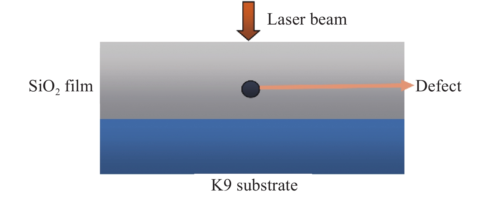
模拟采用的是厚度为250 nm的单层SiO2膜层,基底为K9基底。模拟区域为二维分布,入射激光沿着y轴方向射入包含球形缺陷的单层SiO2膜层中,假定入射激光为电场强度为E0=1 V/m的平面波。在输出端施加完善匹配层(PML)边界条件。模拟的结构如图1所示。

图 1 激光辐照包含缺陷的单层SiO2薄膜示意图
Figure 1. Schematic diagram of single-layer SiO2 film containing defects irradiated by laser
-
首先, 基于时域有限差分算法对比分析了波长为1.064 µm入射激光辐照下单层SiO2薄膜(折射率为nf=1.55)有无缺陷情况下的光场分布。其中缺陷处于膜层表面,缺陷直径为100 nm。结果如图2所示。可以看出,在激光辐照下无缺陷的SiO2薄膜峰值电场出现在膜层表面,电场分布从膜层表面到基底逐渐降低。而当膜层表面存在缺陷时,缺陷诱导膜层电场分布发生变化,峰值电场出现在缺陷和膜层的边界处,电场峰值大约增大了2.3倍。

图 2 缺陷诱导SiO2膜层的光场分布
Figure 2. Light field distribution of SiO2 film induced by defect
-
图3、图4显示了缺陷折射率n0不同时诱导的SiO2膜层光场分布情况。从图3可以看出, 当缺陷的折射率不同时,诱导的膜层峰值电场仍然处于缺陷和膜层的边界处,但峰值电场大小不同。如图4所示,当缺陷的折射率与膜层的折射率相差越大,诱导的电场峰值越大;当缺陷的折射率正好等于膜层的折射率时,峰值电场最小,但仍然高于无缺陷的膜层电场。以上结果说明缺陷在诱导膜层光场增强时具有微透镜效应。当缺陷的折射率与膜层的折射率相差越大,缺陷对入射光的聚焦效应越显著,所以诱导的峰值电场越大。同时当缺陷的折射率等于膜层的折射率时,缺陷仍然诱导光场局部增强。
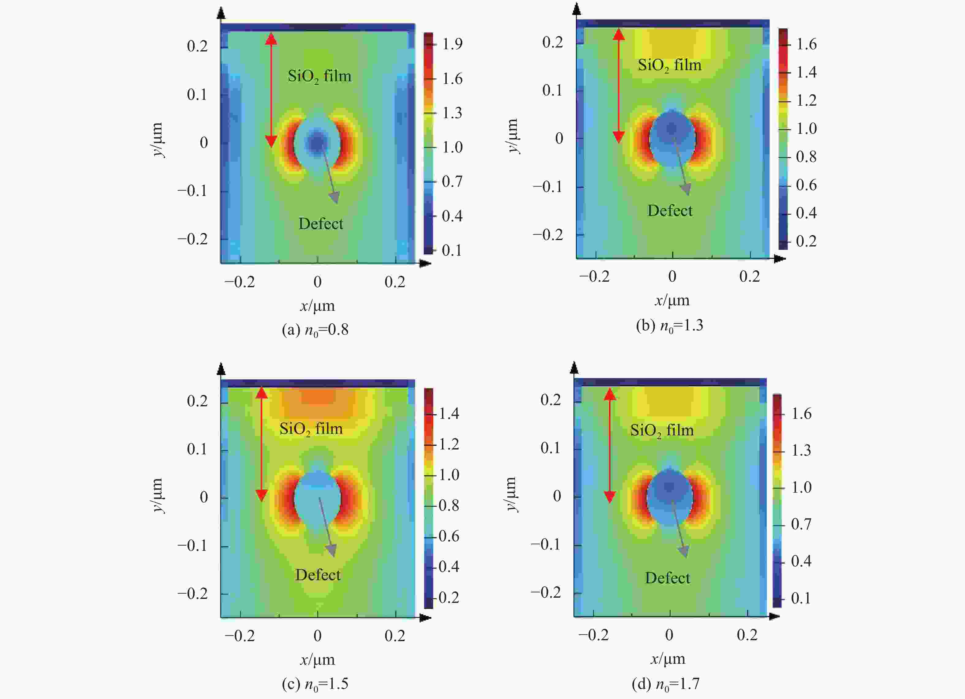
图 3 不同折射率的缺陷诱导SiO2膜层的光场分布
Figure 3. Light field distribution of SiO2 film induced by defect with different refractive index

图 4 膜层的峰值光场对缺陷折射率的依赖关系
Figure 4. Dependence of peak light field on the refractive index of defect
-
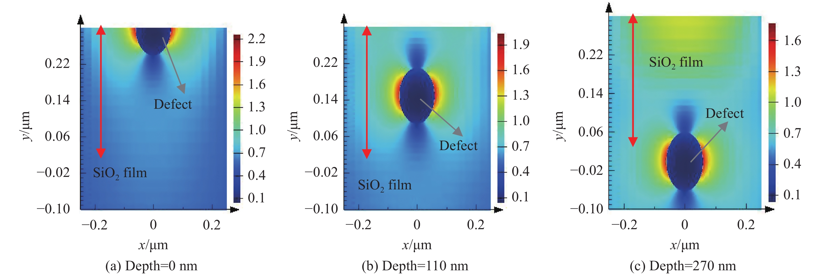
研究显示,缺陷位于膜层的不同位置时,膜层的损伤阈值不同。为此模拟了不同深度的缺陷对膜层光场的影响,如图5所示。可以看出对于同样大小,折射率相同的缺陷,当处于SiO2膜层不同深度时,诱导的膜层峰值电场不同;当缺陷处于膜层表面时诱导的峰值电场最大,随着缺陷的在膜层中深度加大,越靠近基底时,诱导的膜层电场峰值越低。因此处于膜层表面附近的缺陷更容易诱导损伤。
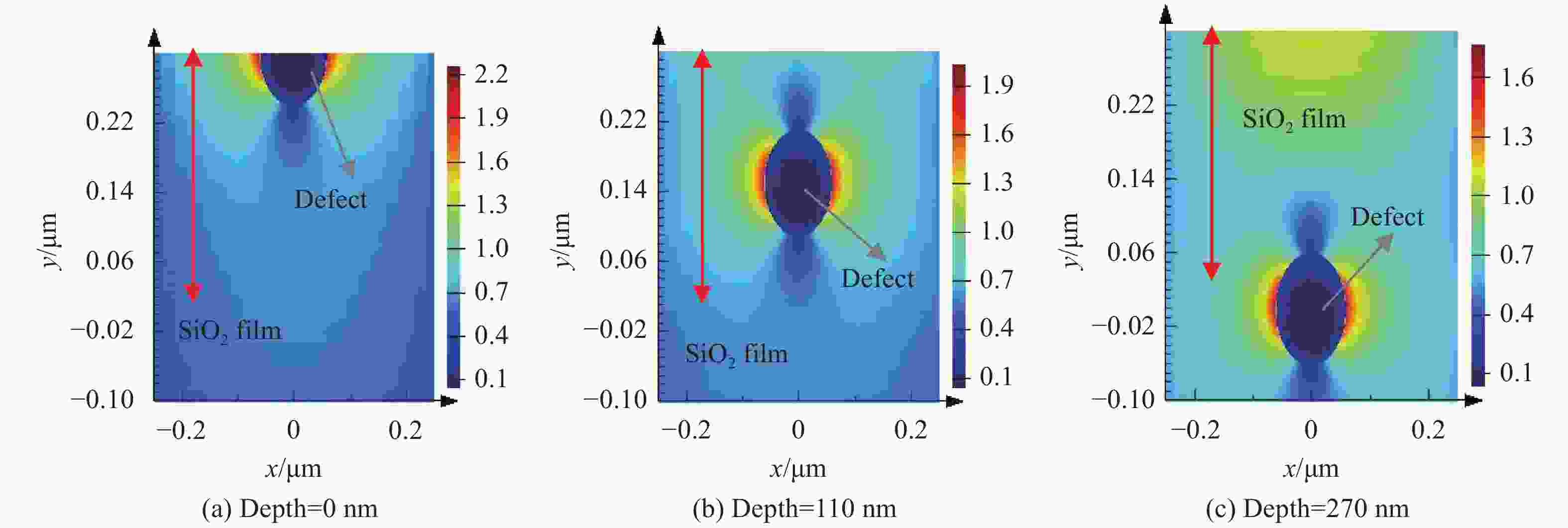
图 5 不同深度的缺陷诱导膜层的光场分布
Figure 5. Light field distribution of films induced by defect with different depths
-
图6为缺陷大小分别为15 、60 、100 nm时膜层光场分布情况。可以看出缺陷尺寸越大诱导的峰值电场越大,因此缺陷尺寸小于膜层厚度的情况下,尺寸较大的缺陷更容易诱导膜层的激光损伤。
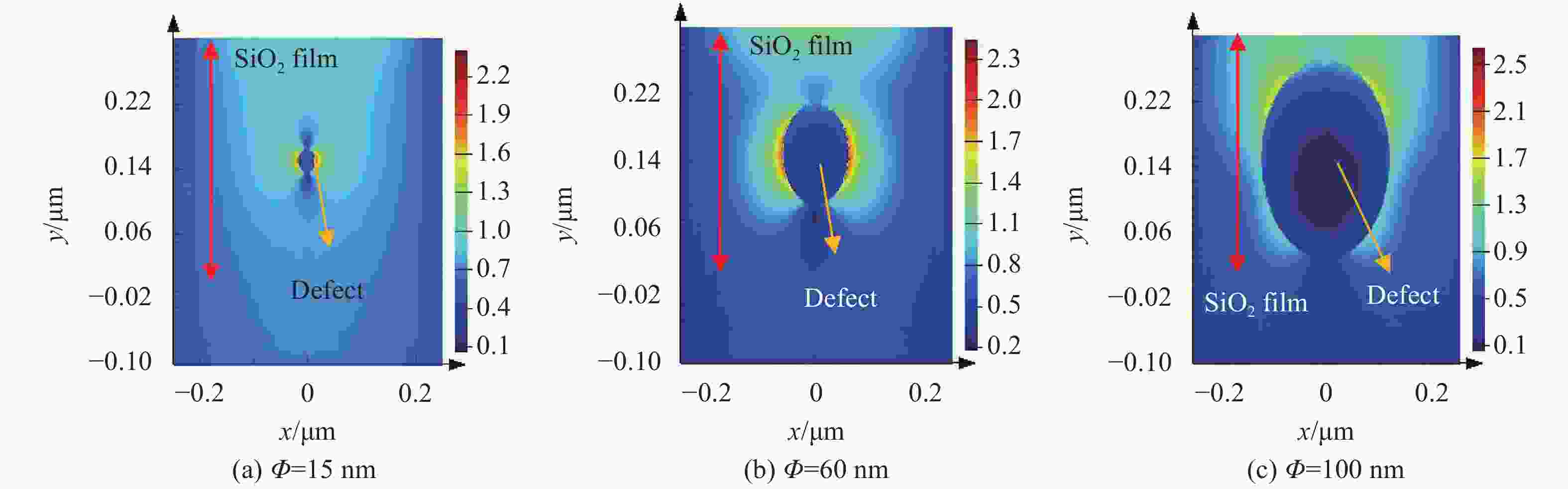
图 6 不同大小的缺陷诱导膜层的光场分布
Figure 6. Light field distribution of films induced by defect with different sizes
-
光学薄膜的激光损伤与入射光波长较大的关系,一般入射光的波长越短,薄膜的损伤阈值越低。图7为SiO2膜层在入射光波长分别为1 064 、532 、355 nm的激光辐照下膜层的光场分布。可以看出,入射光波长越短,缺陷诱导膜层峰值电场越大。所以,当辐照激光的波长越短,薄膜的损伤阈值越低。
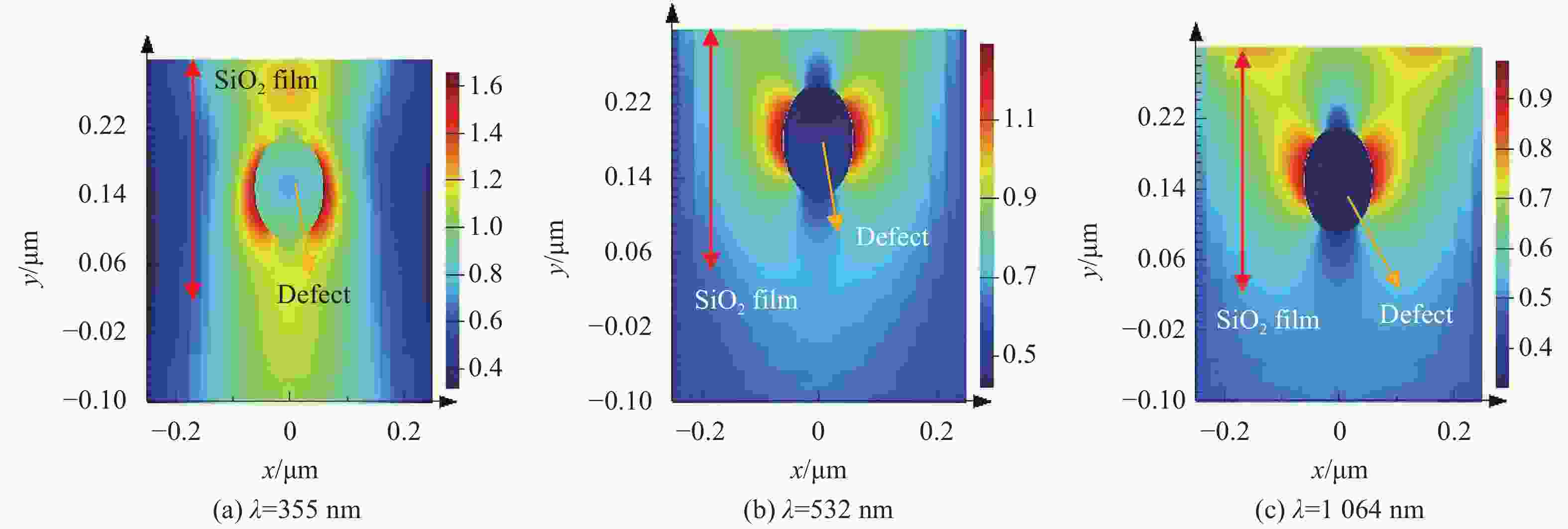
图 7 激光入射波长为355 nm(a)、532 nm(b)、1 064 nm(c)时的光场分布
Figure 7. Light field distribution under laser wavelength of 355 nm (a), 532 nm (b), 1 064 nm (c)
-
光学薄膜的激光损伤,特别是纳秒脉冲激光导致的损伤过程主要还是光学薄膜中各种敏感缺陷引起的损伤。由前面分析可知,缺陷的存在对光学薄膜的光场分布进行了调制,导致光学薄膜局部光场增强,且峰值光场始终位于缺陷与膜层的边界处,因此缺陷与膜层的边界处是薄膜损伤最薄弱的位置。此时光强度为:
$$\begin{split} \\ I=\frac{1}{2}\sqrt{{}^{{{\varepsilon }_{0}}}\!\!\diagup\!\!{}_{{{\mu }_{0}}}\;}{{n}_{i}}{{\left| E \right|}^{2}} \end{split}$$ (1) 所以,缺陷诱导光学薄膜的光场增强会导致缺陷及其周围膜层光强的局部增加。而对于吸收性的缺陷,如金属粒子,杂质缺陷等不仅对其附近光场有调控作用,缺陷诱导光学薄膜的光场增强会导致激光能量沉积的增加,这一关系可以表示为:
$$ Q=\iiint \alpha I{\rm{d}}v $$ (2) 在激光辐照下缺陷会诱导光学薄膜局部光场增强,光场的增强诱导激光能量沉积的增加,进而引起光学薄膜局部温度场的急剧增大,从而诱导光学薄膜热力损伤或等离子冲击爆炸损伤。所以,缺陷诱导光学薄膜的局部光场增强是激光损伤过程是光、热、力等多物理场耦合作用过程的首要过程。
综上所述,在激光辐照下结构性缺陷使得缺陷周围膜层局部光场被调制,导致在激光辐照下缺陷及周围膜层局部光强增强,进而诱导薄膜的损伤;而对于吸收性的缺陷,不仅对其附近光场有调控作用同时由于缺陷的强烈吸收,使缺陷及周围膜层温度场发生显著增加,导致热力损伤或等离子冲击爆炸损伤,最终缺陷处的损伤导致周围膜层的损伤;所以在光学薄膜的激光损伤过程中,缺陷导致光学薄膜局部光场的增强是首要的、第一位的过程,是后续损伤过程的前提。因此,抑制缺陷诱导的光学薄膜的局部光场增强有助于提高光学薄膜的抗激光损伤阈值。
-
文中基于有限差分时域方法分析了缺陷诱导SiO2光学薄膜的光场增强导致的激光损伤。结果显示,缺陷导致SiO2薄膜的光场分布发生变化,无缺陷的SiO2单层薄膜峰值光场位于膜层表面,而有缺陷的SiO2薄膜峰值光场位于缺陷与薄膜的边界处,光场峰值增大了约2.3倍;同时缺陷诱导的光场局部增强不仅依赖于缺陷与膜层之间的相对折射率,而且也依赖于缺陷的大小、缺陷在膜层中的分布深度,以及入射激光波长。缺陷与膜层的折射率越大,缺陷的直径越大,缺陷在膜层中的深度越小,入射激光波长越短,诱导的峰值电场越大。缺陷导致光学薄膜局部光场的增强是光学薄膜激光损伤过程中首要的、第一位的过程,是后续损伤过程的前提。所以抑制缺陷诱导的光学薄膜的局部光场增强有助于提高光学薄膜的抗激光损伤阈值。
Analyses of light field enhancement damage induced by defects in optical thin films
-
摘要:
高损伤阈值的光学薄膜是高功率激光系统的关键器件。众多研究显示,纳米量级的缺陷是光学薄膜激光损伤的主要诱因,是制约光学薄膜向高损伤阈值发展的主要因素。 基于有限差分时域方法分析了纳米大小的缺陷诱导SiO2光学薄膜的局部光场增强导致的激光损伤。结果显示:缺陷的存在使SiO2单层薄膜的光场分布发生了变化,无缺陷的SiO2薄膜峰值光场位于膜层表面,而有缺陷的SiO2薄膜峰值光场位于缺陷与薄膜的边界处,光场增强了约2.3倍;同时缺陷诱导的光场局部增强不仅依赖于缺陷与膜层之间的相对折射率,而且也依赖于缺陷的大小、缺陷在膜层中的分布深度,以及入射激光波长。缺陷与膜层的相对折射率越大,缺陷的直径越大,缺陷在膜层中的深度越小,入射激光波长越短,光场增强越大。研究结果显示光学薄膜中纳米大小的缺陷诱导的光场增强不可忽视,在研究光学薄膜的激光损伤过程中应予以考虑。 Abstract:Optical thin films with high laser-induced damage thresholds are the pivotal components in high power laser systems. A lot of studies have shown that nano defects locating in optical thin films are the main factors which can induce the decreasing of the laser-induced damage thresholds. And, defects have been proved to be the main restrictions in developing optical thin films with the high laser-induced damage thresholds accordingly. Based on the finite-difference time-domain (FDTD) algorithm, the laser-induced damage caused by the local light field enhancement due to the nano defect lodging in SiO2 single layer thin film was analyzed. The modeling results showed that the nano defect caused the changes of light field distribution in SiO2 single layer thin films. For the SiO2 thin film without defect, the peak of light field located on the surface of film layer, whereas the maximum of light field lodged on the boundary between the defect and the film layer when the defect existed in the SiO2 thin film. Moreover, a light field intensification as large as 2.3X in the SiO2 thin film with defect occurred in contrast to the condition of absence of defect. In addition, the local light field intensification induced by defect in optical thin film depended on not only the relative refractive index between the defect and the film layer, but also the defect diameter, the embedded depth of the defect and the wavelength of incident laser. And the larger the relative refractive index between the defect and the film layer, the larger the defect diameter, the shallower the embedded depth of the defect lodging in the film, and the shorter the wavelength of the incident laser are, the stronger the laser field intensifications are. This study can clearly indicate that the light field intensification induced by a nano-defect cannot be neglected, and such nano-defect should be taken into consideration when investigating the laser induced damage of optical thin-films. -
Key words:
- optical thin film /
- defect /
- light field enhancement /
- laser-induced damage
-
图 1 激光辐照包含缺陷的单层SiO2薄膜示意图
Figure 1. Schematic diagram of single-layer SiO2 film containing defects irradiated by laser
图 3 不同折射率的缺陷诱导SiO2膜层的光场分布
Figure 3. Light field distribution of SiO2 film induced by defect with different refractive index
图 4 膜层的峰值光场对缺陷折射率的依赖关系
Figure 4. Dependence of peak light field on the refractive index of defect
图 5 不同深度的缺陷诱导膜层的光场分布
Figure 5. Light field distribution of films induced by defect with different depths
图 6 不同大小的缺陷诱导膜层的光场分布
Figure 6. Light field distribution of films induced by defect with different sizes
-
[1] Liu Z C, Zheng Y, Pan F, et al. Investigation of laser induced damage threshold measurement with single-shot on thin films [J]. Applied Surface Science, 2016, 382: 294-301. doi: 10.1016/j.apsusc.2016.04.093 [2] Demons S G, Staggs M, Minoshima K, et al. Characterization of laser induced damage sites in optical components [J]. Optics Express, 2002, 10(25): 1444-1450. doi: 10.1364/OE.10.001444 [3] Du Y, Liu S, He H, et al. Laser-induced damage properties of antireflective porous glasses [J]. Opt Commun, 2012, 285: 5512-5518. doi: 10.1016/j.optcom.2012.07.120 [4] Jiao H F, Cheng X B, Lu J T, et al. Study for improvement of laser induced damage of 1064 nm AR coatings in nanosecond pulse [J]. Journal of the Optical Society of Korea, 2013, 17(1): 1-4. doi: 10.3807/JOSK.2013.17.1.001 [5] DiJon J, Poiroux T, Desrumaux C. Nano absorbing centers: a key point in the laser damage of thin films[C]// Proc SPIE, 1997: 315-325. [6] Cheng X, Wang Z. Defect-related properties of optical coatings [J]. Advanced Optical Technologies, 2014, 3: 65-90. [7] Cheng X, Shen Z, Jiao H, et al. Laser damage study of nodules in electron-beam evaporated HfO2/SiO2 high reflectors [J]. Appl Opt, 2011, 50: C357-C363. doi: 10.1364/AO.50.00C357 [8] Zhang Longxia, Zhu Xiaobing, Li Fengyu, et al. Laser-induced thermal damage influenced by surface defects of materials [J]. Acta Optica Sinica, 2016, 36(9): 0914001-7. (in Chinese) [9] Papernov S, Schmid A W. Testing asymmetry in plasma-ball growth seeded by a nanoscale absorbing defect embedded in a SiO2 thin-film matrix subjected to UV pulsed-laser radiation [J]. Journal of Applied Physics, 2008, 104(6): 063101. doi: 10.1063/1.2980054 [10] Papernova S, Schmid A W. Two mechanisms of crater formation in ultraviolet-pulsed-laser irradiated SiO2 thin films with artificial defects [J]. Journal of Applied Physics, 2005, 97: 114906. doi: 10.1063/1.1924878 [11] Carr C W, Radousky H B, Rubenchik A M, et al. Localized dynamics during laser-induced damage in optical materials [J]. Physical Review Letters, 2004, 92(8): 087401. doi: 10.1103/PhysRevLett.92.087401 [12] Papernova S, Schmid A W. Correlations between embedded single gold nanoparticles in SiO2 thin film and nanoscale crater formation induced by pulsed-laser radiation [J]. Journal of Applied Physics, 2002, 92: 5720-5728. doi: 10.1063/1.1512691 [13] Xia Z L, Fan Z X, Shao J D. Statistical approach to bulk inclusion initialized damage in films [J]. Optics Communications, 2006, 265(2): 620-627. doi: 10.1016/j.optcom.2006.04.073 [14] Zhu Z, Cheng X, Huang L, et al. Light field intensifification induced by nanoinclusions in optical thin-films [J]. Applied Surface Science, 2012, 258(12): 5126-5130. doi: 10.1016/j.apsusc.2012.01.145 -

 点击查看大图
计量
- 文章访问数: 321
- HTML全文浏览量: 125
- PDF下载量: 36
- 被引次数: 0